SSD_FLASH ADDING USER GUIDE
NOTE:
-
The peripherals specified on this compatible peripheral list (“List”) have been tested by SigmaStar as compatible with SigmaStar’s chip products (“SigmaStar’s Chip”). Please note that SigmaStar tests only the peripheral samples provided by vendors or customers and the foregoing compatibility test results shall apply only to such samples.
-
You could choose at your sole discretion and demand to purchase and use any peripheral on the List with SigmaStar’s Chip. Nevertheless, you should understand that SigmaStar’s compatibility test cannot replace your normal production qualification. Therefore, you should conduct dedicated test in accordance with your normal production qualification procedure prior to using or purchasing such peripherals.
-
You should understand that no warranty of any kind, whether express or implied, is provided by SigmaStar for any peripheral on the List (including, but not limited to, any warranty with regard to the design, production, quality, performance, merchantability, or fitness for a particular purpose of the peripheral). SigmaStar is not liable for any loss, damage, or liability resulted from or relating to the use of any peripheral on the List.
REVISION HISTORY
| Revision No. | Description |
Date |
|---|---|---|
| 1.0 | 10/07/2023 |
1. Using SNI Editor
Open SNI: Version 1.0.9 and above is required.
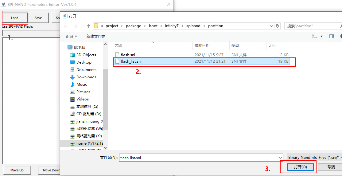
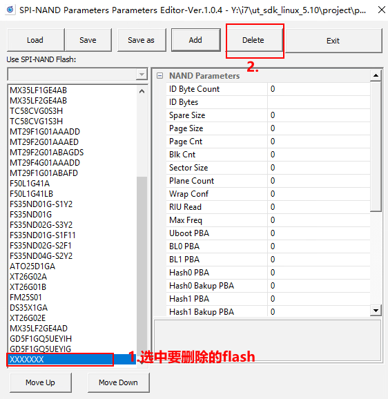
Add Flash:

Delete Flash:
2. Description of Nand Flash Data Structure
2.1. Basic Data Structure
The basic attribute setting interface of Flash is as shown below:

The parameters in the figure and corresponding descriptions are shown in the table below: (Click to Return to Configuration Example)
| Parameter | Description |
|---|---|
| ID Bytes Count | Number of bytes corresponding to the FLASH ID. |
| ID Byte | Used by FLASH ID to identify the Flash (read ID command: 0x9F). |
| Spare Size | Size of oob region. |
| Page Size | Page size, referring to the maximum number of bytes written at a time. |
| Page Count | Number of pages in a block. |
| Block Count | Number of blocks in a Flash device. |
| Sector Size | Unit size used by Flash ECC to calculate ECC check code. |
| Plane Count | Configure to 1 for 2-plane flash, otherwise configure it to 0. |
| Plane Count | Certain Flash features a multi-plane design, and the read and write timing will be slightly different from that of a single-plane design. This parameter is set to 0 by default if no value is filled in. |
| RIU Read | Used to select DMA data transfer or RIU data transfer, DMA data transfer is faster. 0: DMA, 1: RIU. |
| Max Freq | Used to select the clock frequency. 54M is recommended for debugging. In actual application, please confirm the clock frequency according to the flash specification. |
| Uboot PBA | The starting block id of Uboot partition. No need to fill in if there are no special function requirements, the default value is 0. |
| BL0 PBA | The starting position of IPL partition. |
| BL1 PBA | The starting position of IPL backup partition. |
| BAKCNT | The number of backups owned by the IPL partition and the backup partition. |
| Write Protect Offset | The page id corresponding to the partition where Write Protect Table is located. Fill it in according to whether this function is enabled. If function is not enabled, write 0. |
| Vendor Name | Flash Vendor Name |
| Part Number | Flash Part Number (mandatory) |
2.2. Special Data Structure 
2.2.1. Flag Data Structure (Click to Return to Configuration Example)
The special attribute setting interface of Flash is shown in the figure below:
The parameters in the figure and corresponding descriptions are shown in the table below:
| Parameter | Description |
|---|---|
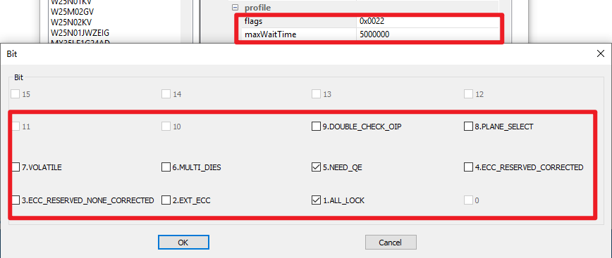
| BIT9 | Special flash needs to determine OIP (busy bit in register) two times. Please check and confirm with the manufacturer. |
| BIT8 | Click for 2-plane special flash. Please query the data sheet or confirm with the manufacturer. |
| BIT7 | Volatile registers, the register value of flash will be checked due to reset cmd or power-off recovery. |
| BIT6 | MULTI_DIES. Fill in according to the data sheet of Flash. |
| BIT5 | NEED_QE. When Flash is performing quad read or quad write, QE bit should be set. |
| BIT4 | ECC_RESERVER (reserved). |
| BIT3 | ECC_RESERVED_NONE_CORRECTED. When ECC_S1 | ECC_S0 is 2b’11, if it means uncorrectable, click. |
| BIT2 | EXT_ECC. Unused. |
| BIT1 | ALL_LOCK. It originally indicated that Flash will be unlocked during initialization. Currently, unlock will be executed regardless of whether it is checked or not. Invalid bit. |
| BIT0 | OTP_AVAIL. Unused. |
| MaxWaitTime | The maximum waiting time for Flash to complete an action, in us, it is recommended to be 10*(Block erase time). |
2.3. Register Data Structure
The register setting interface of Flash is shown in the figure below:

The parameters in the figure and corresponding descriptions are shown in the table below:
| Parameter | Description |
|---|---|
| EccEnabled | ECC enable. After enabling, the ecc function will be turned on to verify and repair data. |
| OtpLock | Lock OTP area. After locking, the OTP area will be read-only. There is no need to fill in if OTP area is unused. |
| OtpEnabled | OTP enable. After enabling, the flash otp area data can be accessed. |
| DieConfig | Die Code, switch die (only required for flash with multi-die structure). |
| Complement | Write-protection related. This parameter is used to complement the write-protected area. |
| TopBottom | Write-protection related. This parameter is used to select the starting address of write-protected area: upper or lower. |
| Blocks | Write-protection related. This parameter is used to select the block of write-protected area. |
| SRP0 | Register protection (unused). |
| SRP1 | Register protection (unused). |
| QeStatus | QE bit related information, to enable QE. This parameter is used to quad read and quad write. |
2.4. Data Operation Structure
Setting interface related to Flash data access is shown in the figure below:
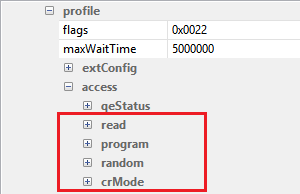
The parameters in the figure and corresponding descriptions are shown in the table below:
| Parameter | Description |
|---|---|
| Read | Read data command configuration, used to modify single read, dual read and quad read. |
| Program | Write data command configuration, used to modify single write and quad write. |
| Random | Write data command configuration (compared with Program, Random will not reset the cache value). |
| CrMode | Cr mode command configuration. For details, please refer to Cr Mode Configuration. |
The composition of all parameters is the same, as shown in the figure below:
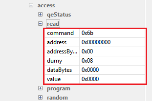
The meaning of each field of the parameters is shown in the following table:
| Parameter | Description |
|---|---|
| Command | Operation command (the 0x6b in the figure is a read operation command). |
| Address | Operation address. If reading and writing do not need to set the address, the read and write register command will need to set the address. |
| Address Bytes | Address length. |
| Dummy | Number of Dummy Cycles, the number of dummy cycles required to be set for timing. |
| Data bytes | Register data length, the length of data that needs to be read or written when reading and writing registers. |
| Value | Register data content, usually the position mask of the corresponding function bit in the register. |
Because all command data structures are shared, some fields might not be required by certain commands. For example, for read and write commands, only command and dummy count need to be set, and the others do not need to be set. For commands to read and write registers, on the other hand, it is necessary to set the command, command address, command address length, and data mask. For details, please refer to the Flash datasheet for flexible adjustments. Next, an example is given to explain in detail how to add a Flash support.
3. NAND Normal Configuration
In the following section, we will take XT26G02E as an example to explain how to find parameters from the datasheet and enter them into SNI.
3.1. Adding a Model
Click the "add" button, enter the Flash model, and click "OK" to add a blank configuration. The operation steps are shown in Figure 3-1:
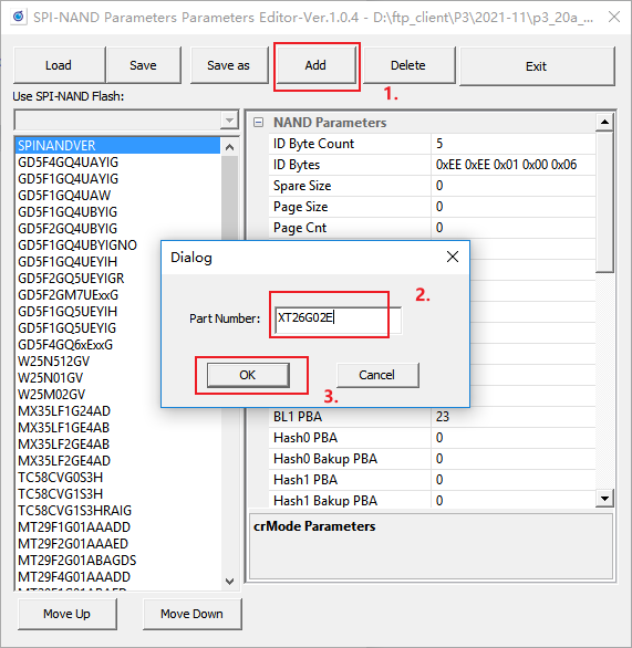
Figure 3-1: Adding Flash Model
3.2. Basic Parameter Configuration 
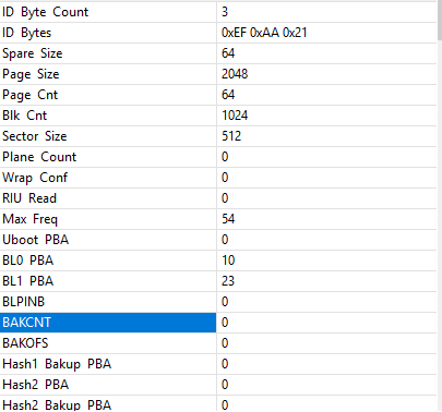
As Figure 3-2 shows, the ID of XT26G02E is two-byte 0x2C 0x24:
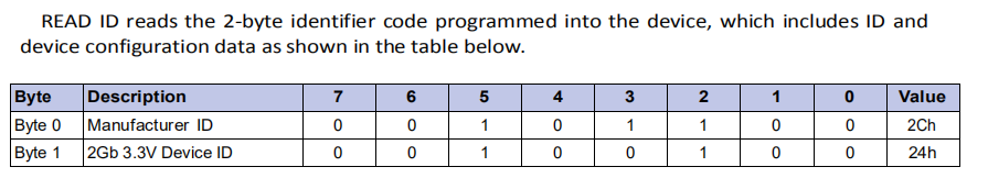
Figure 3-2: XT26G02E ID
Fill in 2 in the ID Byte Count field and 0x2C 0x24 in the ID Bytes field, as shown in Figure 3-3:
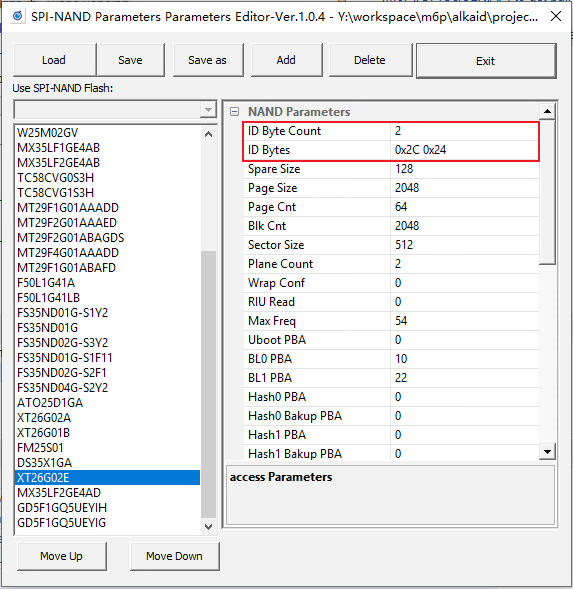
Figure 3-3: NAND Parameter Configuration
As Figure 3-4 and Figure 3-5 show, the page size of XT26G02E is 2048 bytes, each block contains 64 pages, and each page includes a 128-byte empty data area (Spare Size) in addition to the 2048 bytes of valid data. The number of planes is 2, and the total number of blocks is 2048.
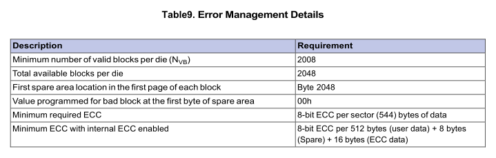
Figure 3-4: Error Management Details
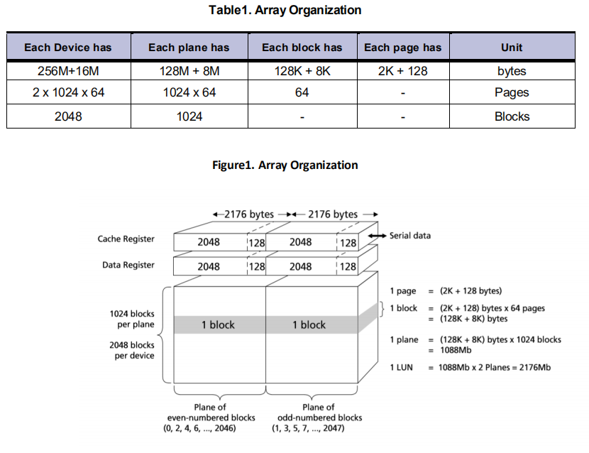
Figure 3-5: Array Organization
Modify SNI accordingly, as shown in Figure 3-6:
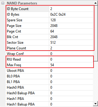
Figure 3-6: SNI Modification
In Figure 3-6, RIU Read indicates whether to use RIU mode. Set it to zero to enable RIU mode, and set it to one to enable DMA mode. Max Freq is the operating frequency of the Flash clock, which should be set according to your need.
Please refer to the corresponding Data Structure for other configurations.
3.3. Special Setting Configuration
3.3.1. Flag Configuration (Click to jump to Special Data Structure)
Double-click the blue area in Figure 3-7, and the configuration interface in Figure 3-8 will pop up:
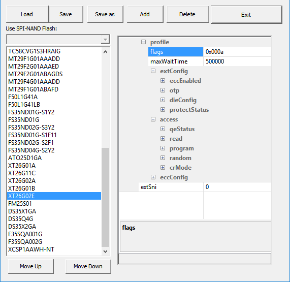
Figure 3-7: Double-Clicking the Blue Area
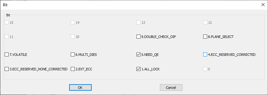
Figure 3-8: Configuration Interface Pop-up
BIT9: As Figure 3-9 shows, when the flash reads and writes data, OIP will be set to 1. Only when OIP is set to 0 can the next operation be performed. Some flashes need to determine that the value of OIP is 0 twice in a row before proceeding to the next step. This feature needs to be confirmed with the manufacturer before you can check this bit.
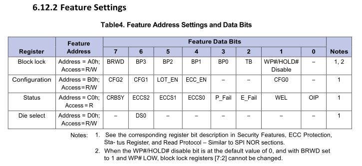
Figure 3-9: Feature Settings
BIT8: As Figure 3-5 shows, when the corresponding flash distinguishes parity blocks, this bit needs to be checked.
BIT7: Volatile is used to indicate whether the QE (Quad Enable) bit in the status register is non-volatile. If it is checked, it is volatile. The value of the QE bit in the volatile status register will lose data and needs to be reset after the system is powered on and off, while the value of the QE bit in the non-volatile status register will retain the original value after the system is powered on and off. However, the non-volatile register has a life limit. Frequent writing to the non-volatile status register will cause the status register to become invalid. The model of Flash in Figure 3-9, for example, does not need to set the QE bit, so this position does not need to be checked.
BIT6: MULTI_DIES indicates whether this model of Flash features multiple-DIE design. According to the description in the data sheet, no description of multiple DIEs was found, so this position is not checked.
BIT5: NEED_QE indicates whether this model of Flash needs to set the QE bit when enabling four-wire mode. As Figure 3-9 shows, we can know that this model of Flash does not need to set the QE bit.
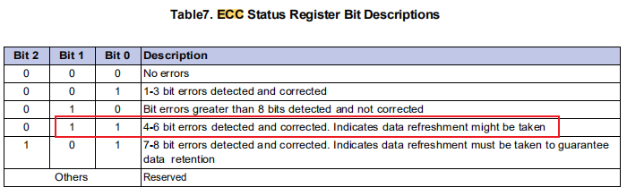
Figure 3-10: ECC Status Register Bit Descriptions
BIT4: ECC_RESERVED_CORRECTED — If ECC status register is 11, then ECC Corrected should be checked.
BIT3: ECC_RESERVED_NONE_CORRECTED — If ECC status register is 11, then ECC Corrected should be checked.
BIT2: EXT_ECC reserved field.
BIT1: ALL_LOCK indicates whether the chip is locked by default. If checked, the driver will automatically unlock. It is recommended to check it by default.
BIT0: OTP_AVAIL reserved field.
3.3.2. MaxWaitTime Configuration Guide
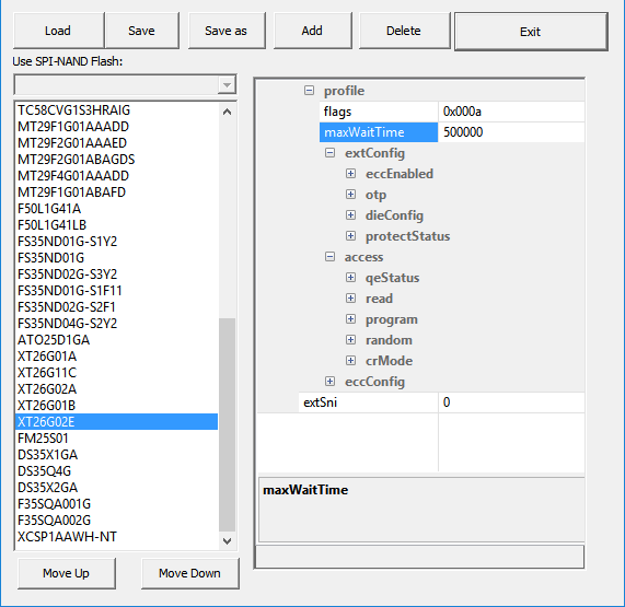
Figure 3-11: MaxWaitTime Parameter Configuration
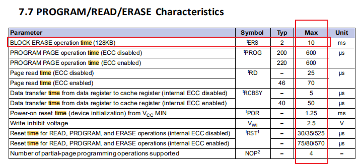
Figure 3-12:PROGRAM/READ/ERASE Characteristics
In Figure 3-11, maxWaitTime indicates the maximum waiting time for reading, writing and erasing. If the success flag has not been detected within the maximum waiting time, the current operation will be exited. Generally the maximum waiting time should be 10 times the maximum timeout time. If the success flag is detected, the operation will be returned immediately. It can be seen, therefore, that increasing the timeout time will not increase the startup time under normal use. As Figure 3-12 shows, the maximum timeout time is 10ms and the time unit of the tool is us, so we should set it to 100000.
3.4. Register Operation Configuration Guide
From Figure 3-13, we can know that the command for this type of Flash to get the status register is 0x0F. Because the commands for reading registers of the various Flashes currently used are the same, the command field can be left blank.

Figure 3-13: GET FEATURES(0Fh) Timing
The corresponding address of the register and the meaning of each bit are shown in Figure 3-14:
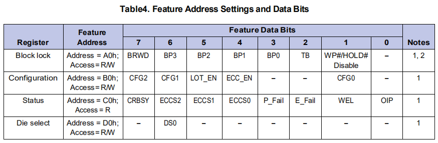
Figure 3-14:Feature Address Settings and Data Bits
As shown in Figure 3-14, the ECC Enable bit is located at Bit 4 of the register with the address 0xB0, so the address is 0xB0. The length of the register is 1-byte, as shown in Figure 3-13, meaning that the value to be filled in the dataBytes field is 0x01. Since there is no dummy clock, the dummy field should be filled in with 0x00. The data length of the register is 1-byte, so the dataBytes field should be filled in with 0x01. The Mask corresponding to Bit 4 is 0x10, so the value field should be 0x10. Fill in 0 for command by default, as Figure 3-15:
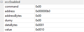
Figure 3-15: EccEnabled Parameter Configuration
Some flash registers still have OTP-related configurations. In such cases, the register addresses where otpLock and otpEnabled are located are 0xB0, and their corresponding masks are 0x80 and 0x40, respectively, while the addressBytes are both 0x01. Command and dummy are 0 by default, as shown in Figure 3-16 and Figure 3-17: Click to jump to description in more details.

Figure 3-16: Configuration Register / Status Register-2 (Address Bxh)
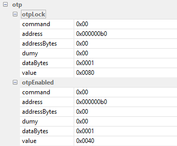
Figure 3-17: OTP Parameter Configuration
3.5. 2 die flash Configuration Guide
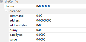
Figure 3-18: die Parameter Configuration
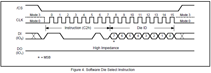
Figure 3-19: Software Die Select Instruction
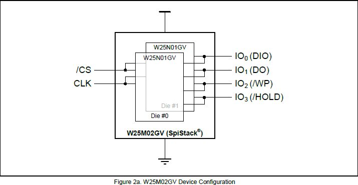
Figure 3-20: W25M02GV Device Configuration
As Figure 3-20 shows, some flashes are composed of two smaller flashes. This type of flash is called 2-die flash. To obtain dieSize, we need to get the size/page size of the smaller flashes. Configuration related to DieCode needs to be configured as shown in Figure 3-19. The command needs to be filled in with 0xC2, the address with 0x01, the addressBytes with 0x01, the dummy with 0x00, and the dataBytes with 0x01. Value does not need to be filled in, as it is controlled by the code.
3.6. Block Status Configuration Guide
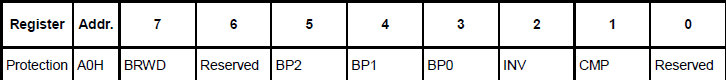
Figure 3-21: Protection Register Bit

Figure 3-22: Complement Parameter Configuration
As Figure 3-21 and Figure 3-22 show, the 0xA0 register of some flashes is saved in CMP bit, which serves the function of write protection. If this bit exists, it needs to be configured, otherwise it will affect writing data to the flash. As shown in Figure 3-21, the configuration corresponding to Figure 3-22 is: command: 0x0 (no configuration required); address: 0xa0; addressBytes: 0x01; dummy: 0x0 (no configuration required); dataBytes: 0x01; value: 0x02.
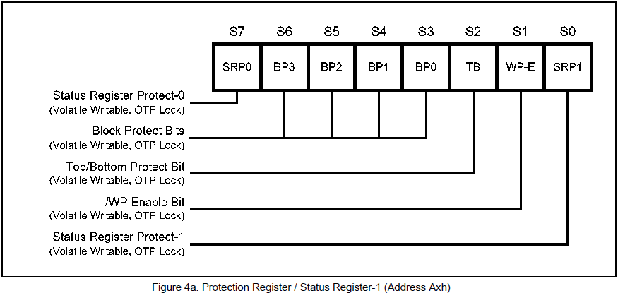
Figure 3-23: Protection Register / Status Register-1 (Address Axh)
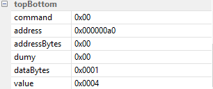
Figure 3-24: TopBottom Parameter Configuration
As Figure 3-23 and Figure 3-24 show, the TB bit exists in the 0xA0 register of some flashes. This bit function is also used for the write protect of the flash. If this bit exists, it needs to be configured, otherwise it will affect the writing of data to the flash. As Figure 3-23 shows, the configuration corresponding to Figure 3-24 is: command: 0x0 (no configuration required), address: 0xa0, addressBytes: 0x01; dummy: 0x0 (no configuration required); dataBytes: 0x01; value: 0x04.
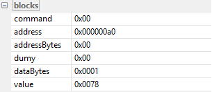
Figure 3-25: Blocks Parameter Configuration
As Figure 3-25 shows, the 0xA0 register of flash has a default value (initial value for power on and off). These values need to be confirmed with the manufacturer. The default value 0xa0 configured in the blocks data structure is used for flash write protect. For configuration information, please refer to: command: 0x0 (no configuration required); address: 0xa0; addressBytes: 0x01; dummy: 0x0 (no configuration required); dataBytes: 0x01; value: (please confirm with the manufacturer).

Figure 3-26: srp Parameter Configuration
As Figure 3-26 shows, the above configuration is related to special functions and does not need to be filled in. If required, RD will help you to fill it in.
3.7. extSni Configuration Guide

Figure 3-27: extSni Parameter Configuration
This data structure needs to be configured when relevant functions are enabled. If no special functions are added, please keep the default value at 0. Please ask our RD to configure it.
3.8. Data Operation Configuration
3.8.1. Reading in Single-Line Mode
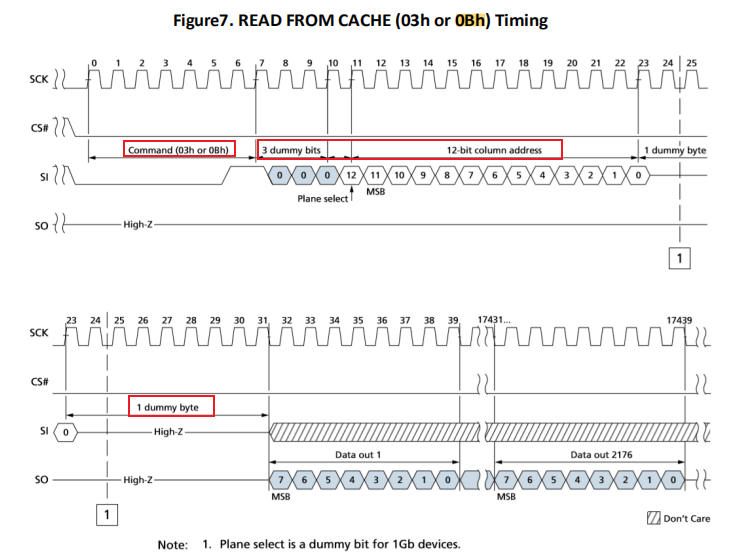
Figure 3-28: READ FROM CACHE (03h or 0Bh) Timing
According to the flash specification, we have the following information:
-
Read Timing: 0x03(command) + 2byte address(addressBytes) + 8 Dummy Cycles(dummy) + data
-
Read Timing: 0x0B + 2byte address + 8 Dummy Cycles + data
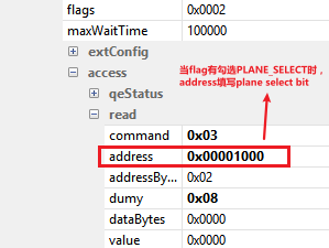
Figure 3-29: Parameter Configuration for 0x03 Read Timing
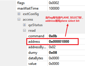
Figure 3-30: Parameter Configuration for 0x0B Read Timing
3.8.2. Reading in Dual-Line Mode
Figure 3-31: READ FROM CACHE x2

Figure 3-32:READ FROM CACHE Dual I/O
According to the flash specification, we have the following information:
-
Read Timing: 0x3B + 2byte address + 8 Dummy Cycles + data
-
Read Timing: 0xBB + 2byte address + 4 Dummy Cycles + data
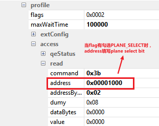
Figure 3-33: Parameter Configuration for 0x3B Read Timing
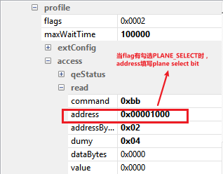
Figure 3-34: Parameter Configuration for 0xBB Read Timing
3.8.3. Reading in Four-Line Mode

Figure 3-35:READ FROM CACHE x4
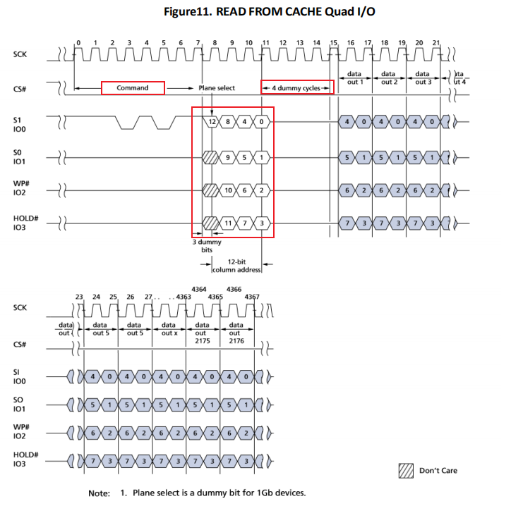
Figure 3-36:READ FROM CACHE Quad I/O
According to the flash specification, we have the following information:
-
Read Timing: 0x6B + 2byte address + 8 Dummy Cycles + data
-
Read Timing: 0xEB + 2byte address + 4 Dummy Cycles + data
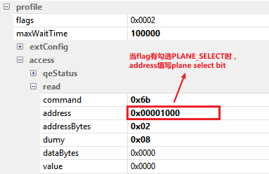
Figure 3-37: Parameter Configuration for 0x6B Read Timing
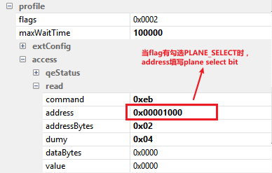
Figure 3-38: Parameter Configuration for 0xEB Read Timing
3.8.4. Writing in Single-Line Mode
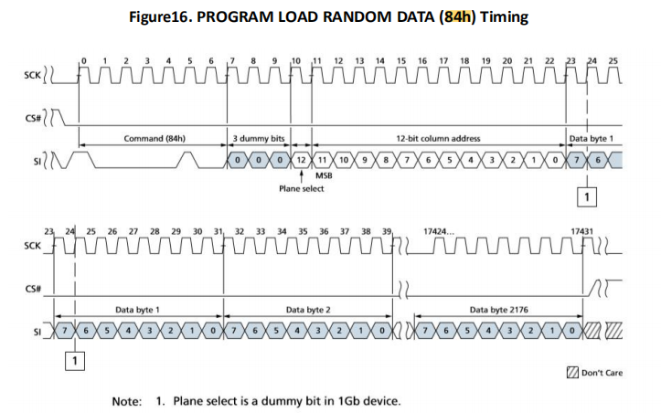
Figure 3-39: PROGRAM LOAD RANDOM DATA (84h) Timing
According to the flash specification, we have the following information:
-
PROGRAM write timing: 0x02 + 2byte address + data
-
RANDOM write timing: 0x84 + 2byte address + data
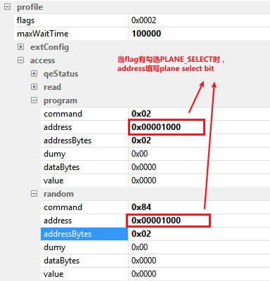
Figure 3-40: Parameter Configuration for 0x02 & 0x84 Write Timing
3.8.5. Writing in Four-Line Mode
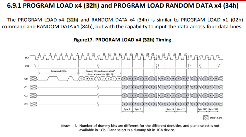
Figure 3-41: PROGRAM LOAD x4 (32h) Timing
According to the flash specification, we have the following information:
-
PROGRAM write timing: 0x32 + 2byte address + data
-
RANDOM write timing: 0x34 + 2byte address + data
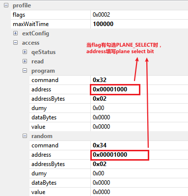
Figure 3-42: Parameter Configuration for 0x32 & 0x34 Write Timing
4. Continuous Read Configuration Guide
Continuous Read mode support: The two modes currently supported are "without BUFF mode" and "BUFF mode"
Without BUFF mode:

Figure 4-1: Continuous Read Mode Without BUFF
Note: The flow has been implemented in the driver. You only need to configure the BUF bit in Sni and read cache command.
Taking W25N01GVxxIG as an example:
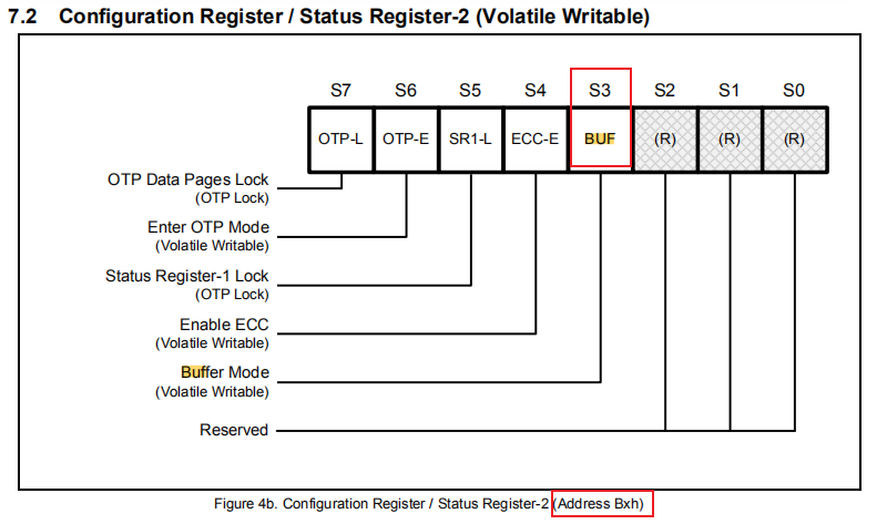
Figure 4-2: Configuration Register / Status Register-2 (Address Bxh)
Four-line reading:
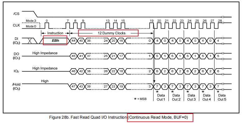
Figure 4-3: Fast Read Quad I/O Instruction (Continuous Read Mode, BUF=0)
According to the flash specification, we have the following information:
-
BUF bit(address :0xB0 Mask:0x08)
-
RANDOM write timing: 0xEB + 2byte address + 8 Dummy Cycles + data
Note: The driver still adopts the method of command + address + dummy + data (here, the address is calculated in 2-byte).

Figure 4-4: Parameter Configuration for crMode
BUFF mode:
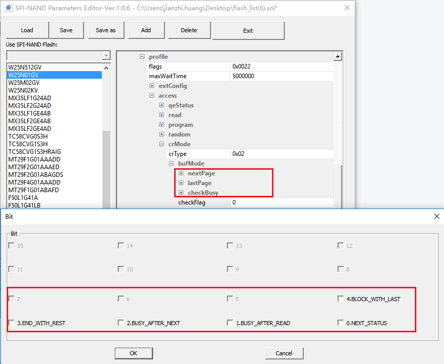
Figure 4-5: Continuous Read Mode With BUFF
| Parameter | Description |
|---|---|
| NextPage Parameters | Command to read the next page. |
| LastPage Parameters | Command to read the last page. |
| CheckBusy Parameters | Used to check the busy status when reading the next or the last page. |
| Parameter | Bit | Description |
|---|---|---|
| BLOCK_WITH_LAST | BIT4 | Checked if the continuous read cannot exceed one block |
| END_WITH_REST | BIT3 | Checked if reset is required at the end of continuous read |
| BUSY_AFTER_NEXT | BIT2 | Checked if CheckBusy is required when reading the next page. Note that CheckBusy Parameters should be filled in. |
| BUSY_AFTER_READ | BIT1 | Checked if CheckBusy is required when reading the last page. Note that CheckBusy Parameters should be filled in. |
| NEXT_STATUS | BIT0 | Checked if CheckBusy is required when reading the next page. (The check here refers to OIP.) |
Taking GD5F1GQ4UEYIH as an example:

According to the flash specification, we have the following information:
-
Next Page command: 0x31
-
Last Page command: 0x3F
-
When reading the next page, it is required to: check OIP
-
Continuous read cannot exceed one block

5. Check ECC Configuration Guide
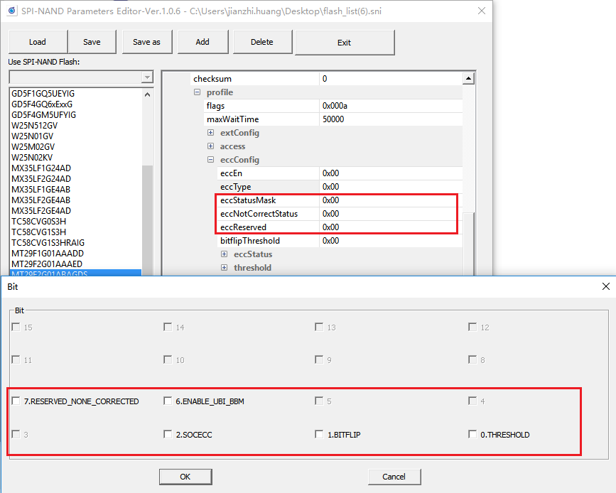
Figure 5-1: Parameter Configuration for Check ECC
Table 5-1: eccConfig Parameter Description
| Parameter | Description |
|---|---|
| eccEn | Whether to enable customized ecc check. |
| eccType | Check several special settings related to ecc, please refer to Table 5-2. |
| eccStatusMask | Ecc valid status bit. |
| eccNotCorrectStatus | The ecc status value indicating that the error cannot be corrected. |
| eccReserved | When RESERVED_NONE_CORRECTED is selected for eccType, it also means the ecc status value indicating that the error cannot be corrected. |
| BitflipThreshold | Set a threshold for the number of corrected bits, which is used for bbm. If bbm is not used, it can be ignored. |
Table 5-2: Bit Parameter Description
| Parameter | Bit | Description |
|---|---|---|
| RESERVED_NONE_CORRECTED | BIT7 | Check if there are two states in the ecc status value indicating ecc error. |
| ENABLE_UBI_BBM | BIT6 | Check if UBI_BBM is enabled (The function of UBI BBM is to rewrite the data to other data blocks when correctable data is found to prevent data damage. If used, please use the bit flip mechanism or threshold mechanism according to the flash used to prevent frequent data rewriting). |
| SOCECC | BIT2 | Driver use, no need to check. |
| BITFLIP | BIT1 | If you choose to use the bit flip mechanism, check it. |
| THRESHOLD | BIT0 | If you choose to use the threshold mechanism, check it. |
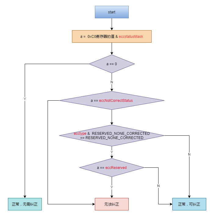
Figure 5-2: Debug Flow
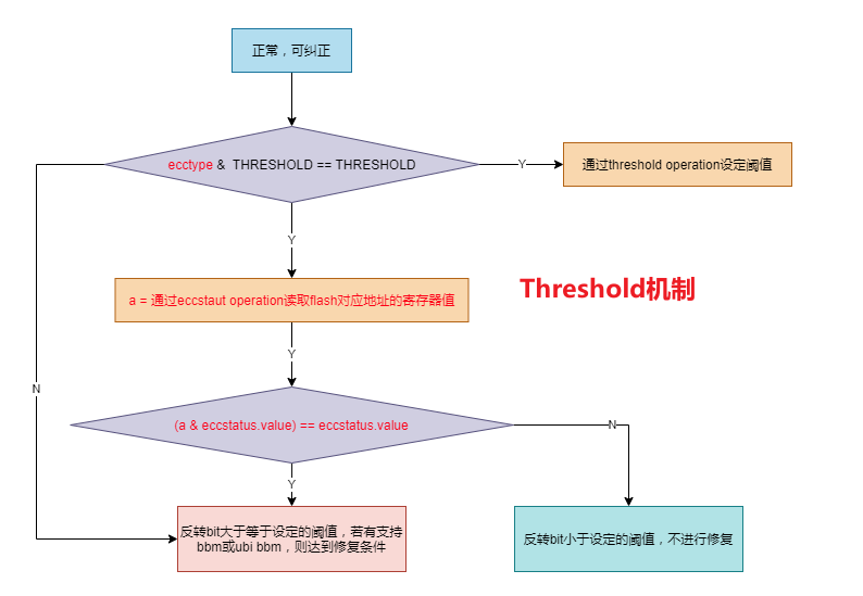
Figure 5-3: Debug Flow for Threshold Mechanism
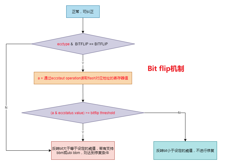
Figure 5-4: Debug Flow for Bit flip Mechanism
Taking GD5F1GQ4xExxH as an example:
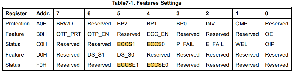
Figure 5-5: Features Settings
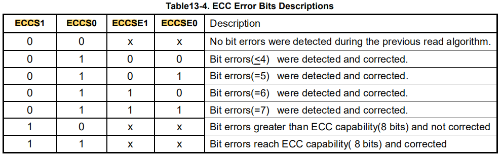
Figure 5-6: ECC Error Bits Descriptions
According to the flash specification, we have the following information:
-
ECCS1 and ECCS0 are used to indicate ecc status, while ECCSE1 and ECCSE0 are used to indicate how many bit flips have occurred.
-
bit flip mechanism is applicable.
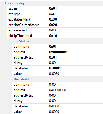
Figure 5-7: Parameter Configuration for GD5F1GQ4xExxH ECC
Taking TC58CVG0S3HxAIx as an example:
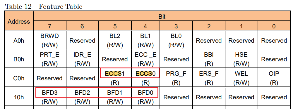
Figure 5-8: Feature Table

Figure 5-9: Feature Table - C0h Address Description
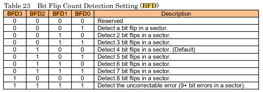
Figure 5-10: Bit Flip Count Detection Setting (BFD)
According to the flash specification, we have the following information:
-
ECCS1 and ECCS0 are used to indicate ecc status.
-
When the value of ECCS1 and ECCS0 is equal to 0x30, it means that the bit flip exceeds the set threshold.
-
BFD3 ~ 0 are used to set threshold.
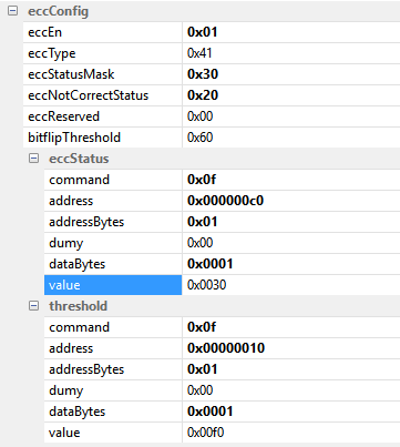
Figure 5-11: Parameter Configuration for TC58CVG0S3HxAIx ECC
6. Readid Configuration Guide
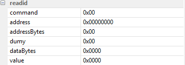
Figure 6-1: Parameter Configuration for Readid
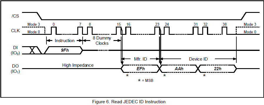
Figure 6-2: Read JEDEC ID Instruction
For some flashes, the timing of reading IDs is different from the figure above and does not require 8 dummies. When this problem occurs, you need to fill in the data structure, otherwise there is no need to fill in. Example — command: 0x9f; address: 0x0; addressBytes: 0x0; dummy: 0x0; dataBytes: 0x0; value: 0x0.
7. InitSet Configuration Guide
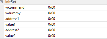
Figure 7-1: Parameter Configuration for InitSet
Some flashes may need to be written twice to access register data. For example, when a flash from a DS manufacturer operates on the 0xa0 register, it needs to write 0x02 to the 0xa0 register first before it can write data to the 0xa0 register. Please confirm this feature with the manufacturer. If the above scenario applies to you, you may ask rd to help fill in the relevant data. In addition, this data structure can also be used for other operations related to flash register configuration. There is no need to fill in the data unless there are special requirements.
8. OTP Operation Configuration Guide
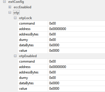
Figure 8-1: Parameter Configuration for otp
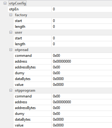
Figure 8-2: Parameter Configuration for otpConfig
Table 8-1: Parameter Description of otp
| Parameter | Description |
|---|---|
| otpEn | Whether to enable otp function. |
| Factory | Set the starting position and length of factory area. Because the otp of nand flash is based on page, the units of start and length are pageID * page size. |
| User | Set the starting position and length of user area. Because the otp of nand flash is based on page, the units of start and length are pageID * page size. |
| Otpread | Read otp operation. |
| Otpprogram | Program otp operation. |
| Otplock | Lock the otp area. Once locked, the otp area can no longer be edited. |
| Otpenable | Enable otp mode. Any otp related operation requires switching the flash working mode to otp mode. |
Taking W25N01GVxxIG/IT as an example:
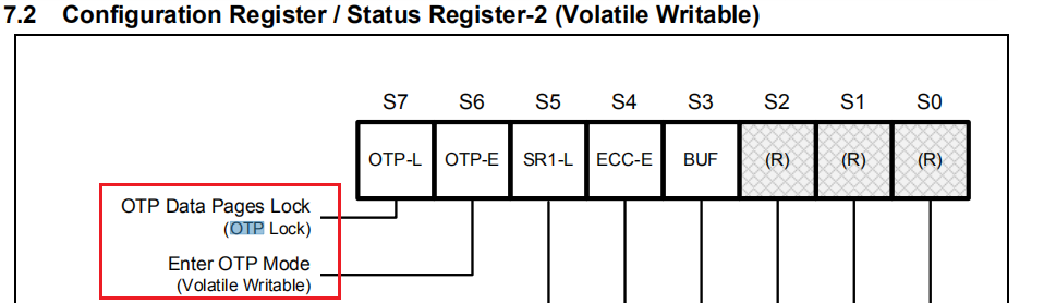
Figure 8-3: Configuration Register / Status Register-2 (Volatile Writable)
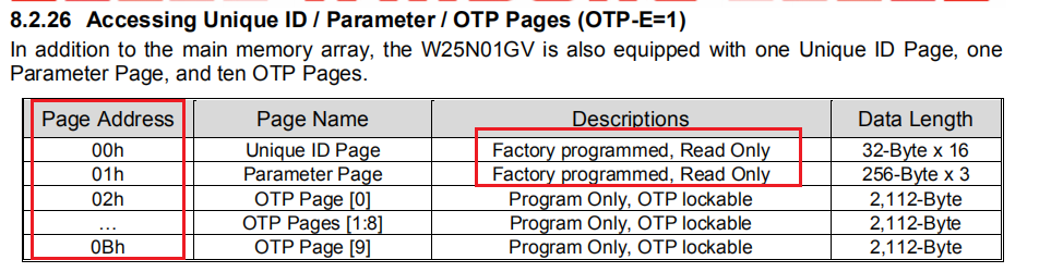
Figure 8-4: Accessing Unique ID / Parameter / OTP Pages (OTP-E=1)

Figure 8-5: Read Operations & Program and OTP Lock Operations
According to the flash specification, we have the following information:
-
Register location where OTP_E and OTP_L bits are located.
-
Factory is page0 ~ 1, user is page2 ~ B.
-
The operation of Otp read program is the same as normal reading and writing, and continue read is not supported.
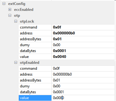
Figure 8-6: Parameter Configuration for W25N01GVxxIG/IT otp
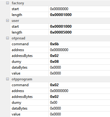
Figure 8-7:Parameter Configuration for W25N01GVxxIG/IT otp
(Click here to return to Register Configuration Guide)
9. Nor Flash Dara Structure Description (Applicable to SSD210/212/222X/9211X)
9.1. Basic Data Structure
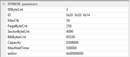
Figure 9-1: Parameter Configuration for SPINOR
Table 9-1: Parameter Description of SPINOR
| Parameter | Description |
|---|---|
| FLASH ID | Used to identify flash (such as read ID command: 0x9F). |
| Max Clk | Select CLK speed, 54M is recommended during debugging. Please confirm the actual application according to the flash specification. |
| Page Byte Count | Page length, the maximum number of bytes written in a single time. |
| Sector Byte Count | Number of bytes in Sector erase. |
| Block Byte Count | The number of bytes in Block erase (such as command: 0xD8). |
| Capacity | Total Flash size. |
| Max Wait Time | The maximum waiting time for flash to complete an action, unit us, recommended 10* (Block erase time). |
| ExtSni | Enable special function. Please fill in 0 as the default value. |
9.2. Advanced Data Structure
The advanced attribute setting interface of the software is shown in Figure 9-2:

Figure 9-2: Advanced Attribute Setting Interface
The meanings of read-related attributes are shown in Table 9-2:
Table 9-2: Read-Related Attribute Description
| Parameter | Description |
|---|---|
| Complement parameter | Select write protection mode. |
| TopBottom parameter | Used to select top mode or bottom mode for write protection. |
| Blocks parameter | Write protection parameters. Please refer to the write protection chapter in data sheet for details. |
| SRP0 parameter | Register protection (reserved). |
| SRP1 parameter | Register protection (reserved). |
| rQuadEnable parameter | Enable four-wire mode. |
The meanings of write-related attributes are shown in Table 9-3:
Table 9-3: Write-Related Attribute Description
| Parameter | Description |
|---|---|
| Complement parameter | Select write protection mode. |
| TopBottom parameter | Used to select top mode or bottom mode for write protection. |
| Blocks parameter | Write protection parameters. Please refer to the write protection chapter in data sheet for details. |
| SRP0 parameter | Register protection (reserved). |
| SRP1 parameter | Register protection (reserved). |
| rQuadEnable parameter | Enable four-wire mode. |
Note: If you fill in rQuadEnable or wQuadEnable, you need to set needQE to 0x01.
| Parameter | Description |
|---|---|
| ReadData parameter | Setting related to reading data. |
| Program parameter | Setting related to writing data. |
The composition of all parameters is the same, as shown in Figure 9-3:
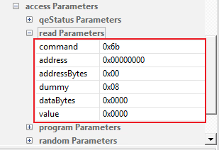
Figure 9-3: Parameter Composition
The meaning of each field of parameter is shown in Table 9-4:
Table 9-4: Parameter Description
| Parameter | Description |
|---|---|
| Command | Operation command (0x6b in the picture is the read operation command) |
| Address | Operation address. Reading and writing do not need to set the address, but reading and writing register commands need to set the address. |
| Address Bytes | Address length. |
| Dummy | The number of Dummy Cycle as required to be set by timing. |
| Data bytes | The length of register data, that is, the length of data that needs to be read or written when reading or writing registers. |
| Value | The content of register data. This field is usually filled in with the location mask of the corresponding function in register. |
Because all command data structures are shared, some fields are not required for certain commands. For read and write commands, for instance, only the commands and dummy count should be set, while others do not need to be set. The command to read and write the register, however, requires setting the command, command address, command address length, and data mask (mask). For details, you can refer to the Flash data manual for flexible adjustments. The next chapter provides an example explaining how to add Flash support in detail.
10. NOR Normal Configuration Guide
In the following, we will take XT26G02E as an example to explain how to find parameters from the datasheet and enter them into SNI.
10.1. Adding a Model
Click the "add" button, enter the Flash model, and click "OK" to add a blank configuration. The operation steps are shown in Figure 10-1:
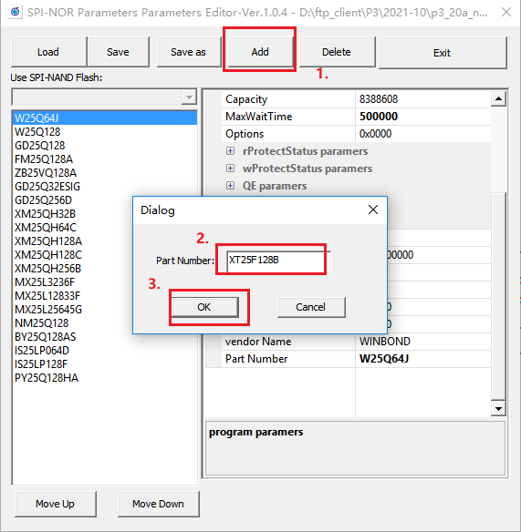
Figure 10-1: Adding a Model
10.2. Basic Data Structure Configuration Guide
As Figure 10-2 shows, the ID of XT26G02E is 0x0B 0x40 0x18:
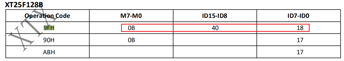
Figure 10-2: XT25F128B ID
As Figure 10-3 shows, you can see the basic size information of Flash.
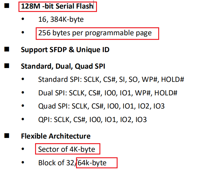
Figure 10-3: The Basic Size Information of Flash
As Figure 10-4 shows, the maximum timeout time that can be obtained is 1.5 seconds:

Figure 10-4: Obtaining Time Table
Based on all the data that can be obtained, modify the parameter settings as shown in Figure 10-5:
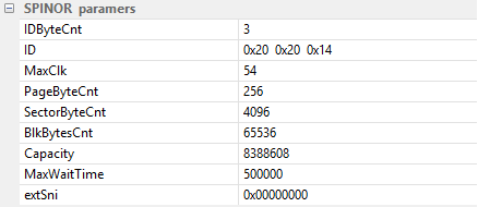
Figure 10-5: XT26G02E Parameter Configuration
10.3. Instructions on Data Structure Configuration Operated by Register
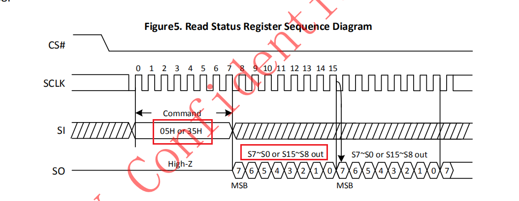
Figure 10-6: Read Status Register Sequence Diagram
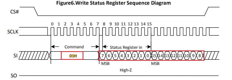
Figure 10-7: Write Status Register Sequence Diagram
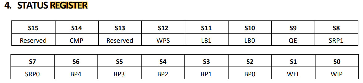
Figure 10-8: STATUS REGISTER
Similar to SPINAND Flash, the following information can be obtained as Figure 10-6, Figure 10-7, and Figure 10-8 show:
-
To read S7-0, use command: 0x05
-
To read S15-8, use command: 0x35
-
To write S15-0, use command: 0x01
-
CMP: bit14
-
Block lock: bit6-2
-
SRP1: bit8
-
SRP0: bit7
-
QE: bit9
Modify the setting as the following figures show:
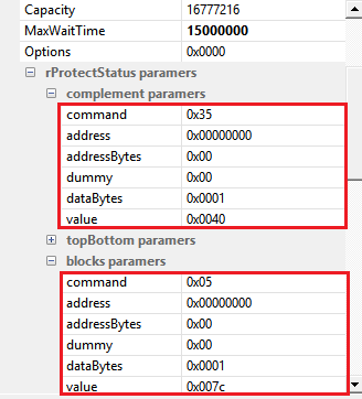
Figure 10-9: Configure Register Parameter
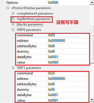
Figure 10-10: Configure Register Parameter
When SPINOR Flash reads register command, it will only return one byte, while two bytes will be written at the same time when writing. When reading, you need to know what the two-byte read command is when writing. You can double-click the dialog box configuration that pops up in the address field, as Figure 10-11 shows:
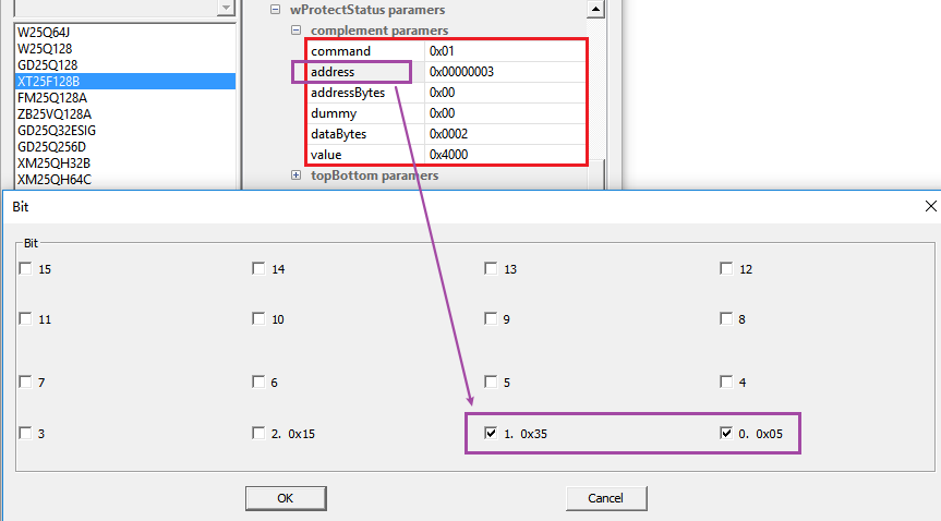
Figure 10-11: Obtain Read Command
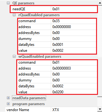
Figure 10-12: Configure Register Parameter
10.4. Description of Data Operation Data Structure
10.4.1. Reading in Single-Line Mode
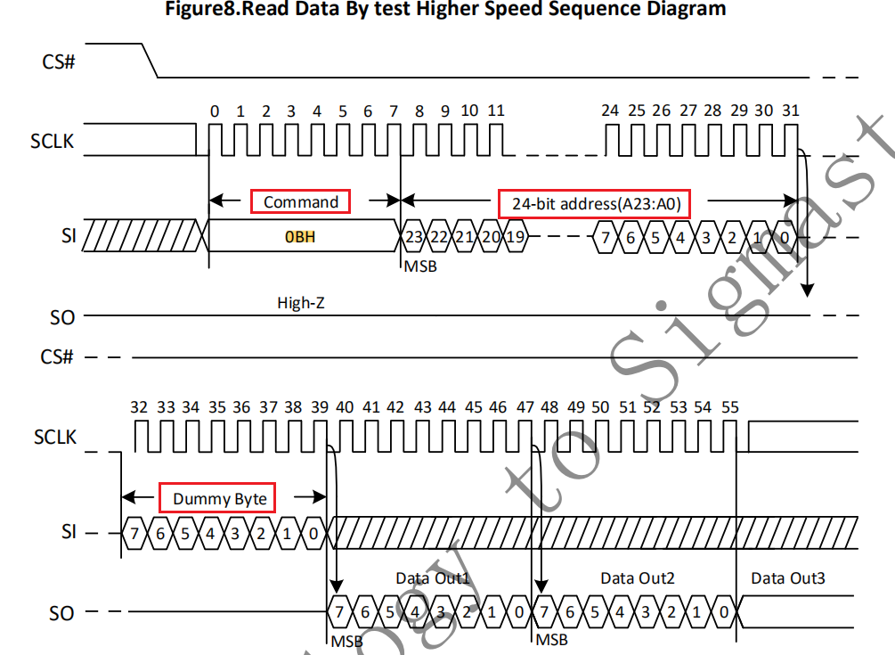
Figure 10-13: Read Data By test Higher Speed Sequence Diagram
According to the flash specification, we have the following information:
- Read Timing is: 0x0B + 3byte address + 8 Dummy Cycles + data

Figure 10-14: Parameter Configuration for Single-Line Read Timing
10.4.2. Reading in Dual-Line Mode
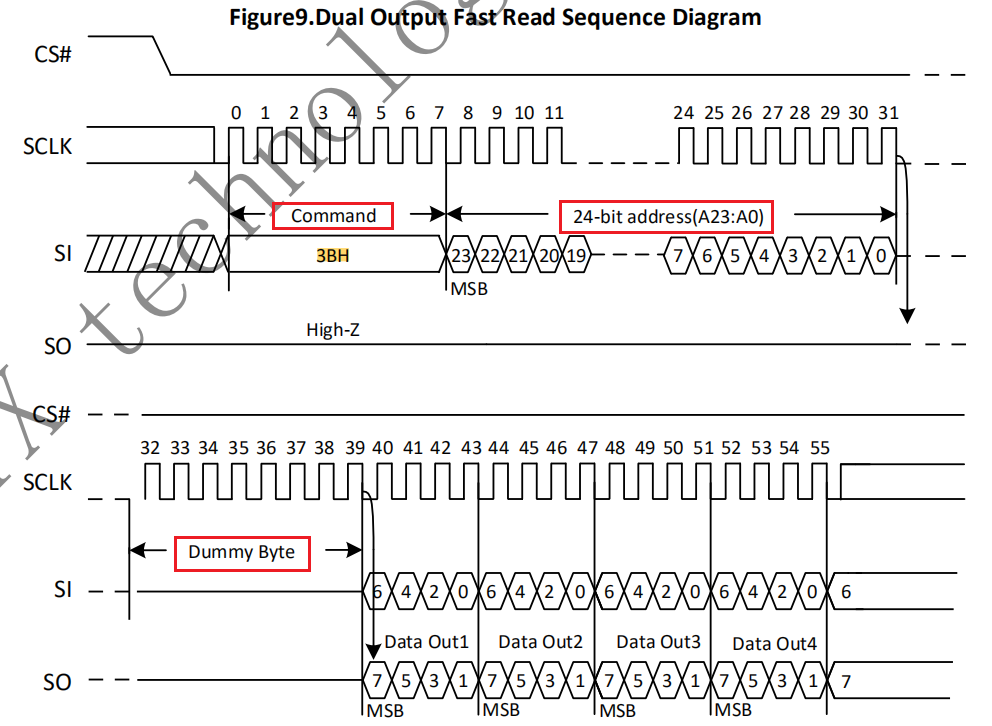
Figure 10-15: Dual Output Fast Read Sequence Diagram
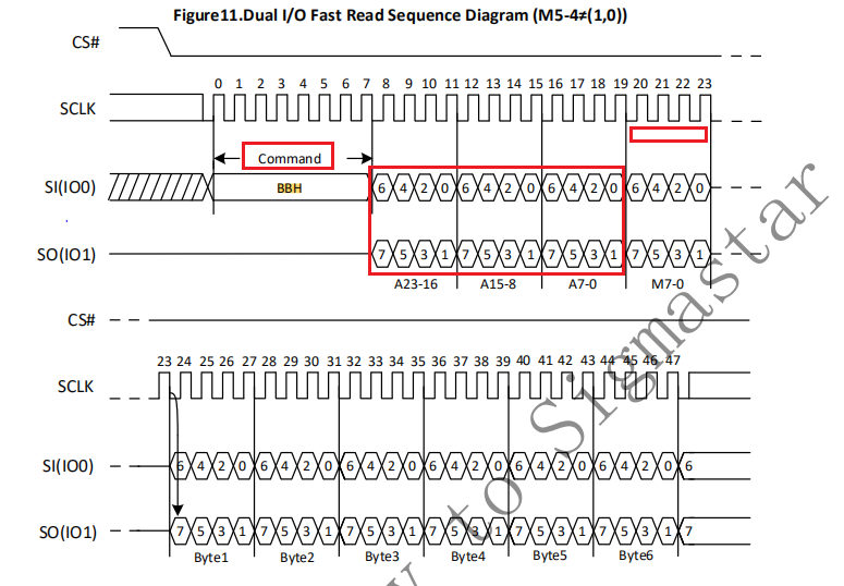
Figure 10-16: Dual I/O Fast Read Sequence Diagram
According to the flash specification, we have the following information:
-
Read Timing is: 0x3B + 3byte address + 8 Dummy Cycles + data
-
Read Timing is: 0xBB + 3byte address + 4 Dummy Cycles + data
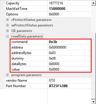
Figure 10-17: Parameter Configuration for 0x3B Read Timing
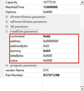
Figure 10-18: Parameter Configuration for 0xBB Read Timing
10.4.3. Reading in Four-Line Mode
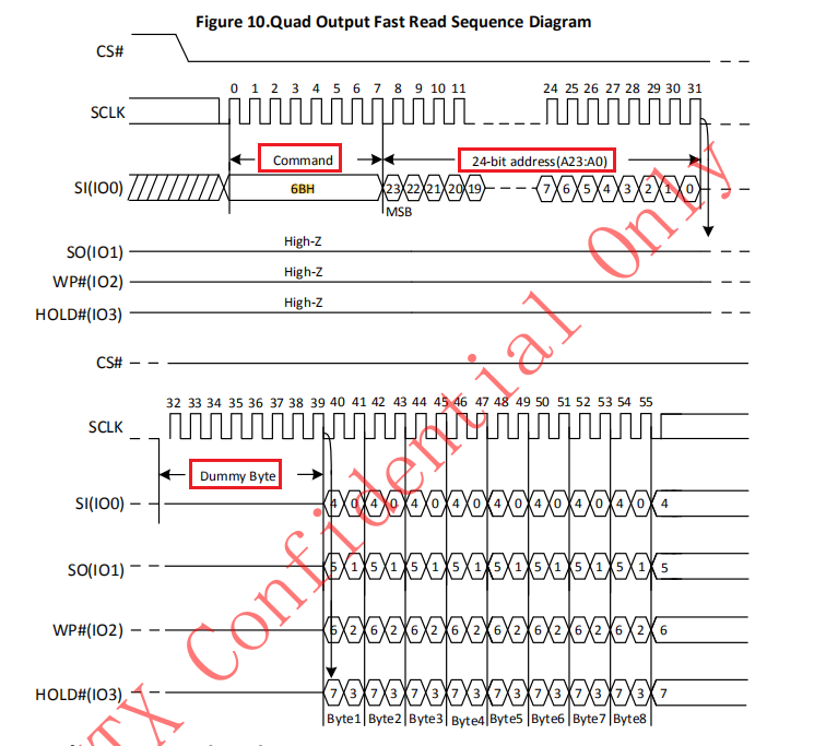
Figure 10-19: Quad Output Fast Read Sequence Diagram
According to the flash specification, we have the following information:
- Read Timing is: 0x6B + 3byte address + 8 Dummy Cycles + data
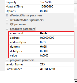
Figure 10-20: Parameter Configuration for 0x6B Read Timing
10.4.4. Writing in Single-Line Mode
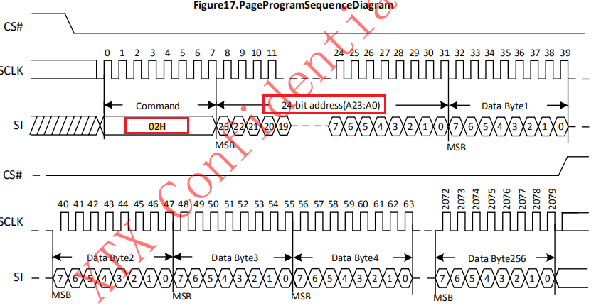
Figure 10-21: Page Program Sequence Diagram
According to the flash specification, we have the following information:
- PROGRAM write timing: 0x02 + 3byte address + data
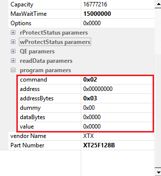
Figure 10-22: Parameter Configuration for 0x02 Write Timing
10.4.5. Writing in Four-Line Mode
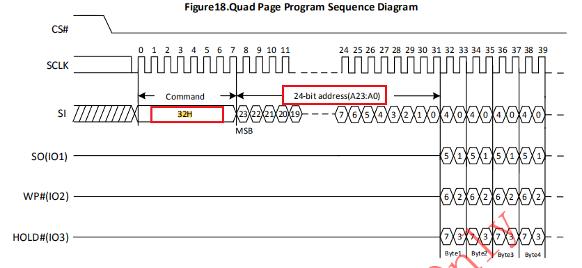
Figure 10-23: Quad Page Program Sequence Diagram
According to the flash specification, we have the following information:
- PROGRAM write timing: 0x32 + 3byte address + data
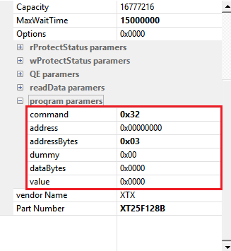
Figure 10-24: Parameter Configuration for 0x32 Write Timing