SSD_DISP Panel Lighting Reference
1. Basic introduction
1.1. Overview
This document mainly explains the configuration and use related to the panel lighting.
1.2. Chip related specifications
| Specification Chip |
TTL | MIPI | SPI | SRGB | HDMI |
|---|---|---|---|---|---|
| 201/202 | Supported | Supported | Supported | ||
| 21X/22X | Supported | Not Supported | Supported | Supported | Not Supported |
| 203 | Not Supported | Not Supported | Supported | Not Supported | Supported |
1.3. Keyword Description
-
TTL/MIPI/SRGB (SSD20X does not support SRGB)
These are the LCD Panel interface.
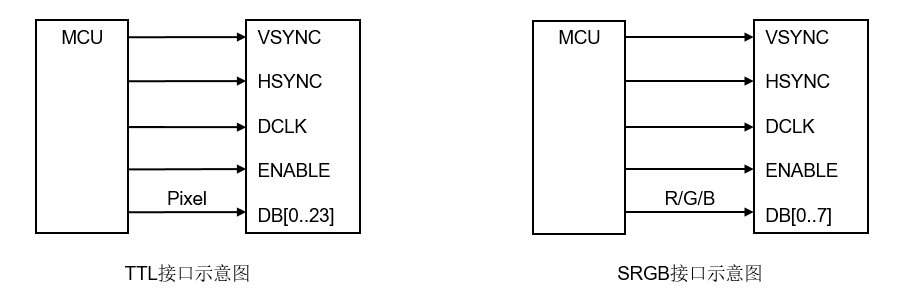
The TTL interface signal type is TTL level, the content of the signal is RGB565 or RGB666 or RGB888, horizontal and vertical synchronization (HSYNC/VSYNC), clock (CLK) and data valid signal (DE).
The MIPI interface signal type is LVDS signal, and the content of the signal is video stream data and control instructions.
The SRGB interface divides the RGB data of one pixel into three transmissions to the panel.
-
HDMI
High Definition Multimedia Interface is a fully digital video and sound transmission interface that can transmit uncompressed audio and video signals.
2. TTL panel lighting
2.1. Specifications
| Specification Chip |
Maximum Resolution | Signal Format |
|---|---|---|
| 201/202 | 1280x720 60fps | RGB565/RGB666/RGB888 |
| 21X/22X | 1280x720 60fps | RGB565/RGB666/RGB888 |
| 203 | Not supported | Not supported |
2.2. Basic Concepts
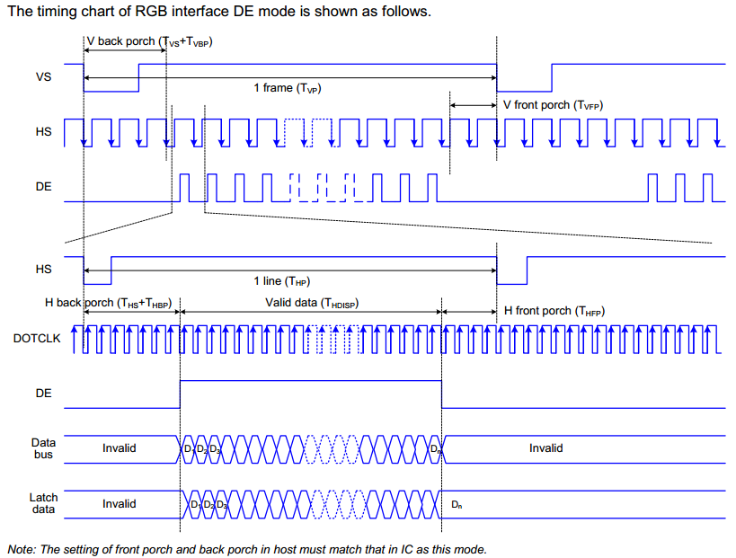
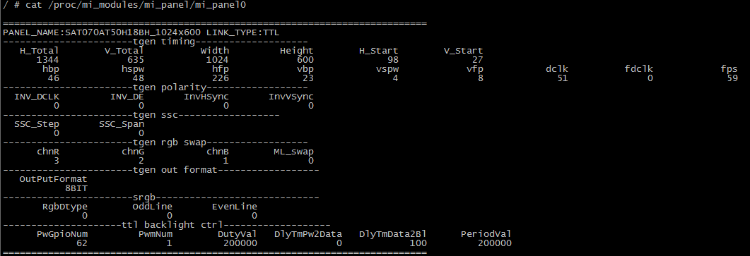
There are two types of Parallel RGB Interface, DE mode and HV mode. When DE mode is enabled, VSYNC, HSYNC, DOTCLK, DE, D[0-23] pins are used. When HV mode is enabled, VSYNC, HSYNC, DOTCLK, D[0-23] are used. Now the program uses DE mode by default, please configure relevant parameters according to DE mode.
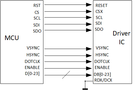
Some panel driver ICs need to be initialized, which is actually the setting of their internal register, which is usually communicated through the SPI or IIC interface. The cmd and data required for initialization are generally provided by the panel factory, and the data format when sending needs to refer to the panel datasheet.
Panels using Parallel RGB Interface require HSYNC, VSYNC, and DOTCLK as synchronization signals, and RGB data is only valid in a specific interval of timing.
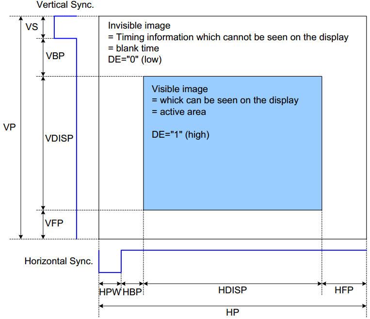
The blanking interval in the line and field signals is an invisible area. Only the RGB data in the active interval will be finally displayed. Different panel Driver ICs have different requirements for the blanking interval.
In line signal:
Htotal = HSYNC + HBP + HFP + H Active
In field signal:
Vtotal = VSYNC + VBP + VFP + V Active
Finally calculate the pixel clock frequency:
Pixel CLK = Htotal * Vtotal * fps
The configuration related to the timing in the Panel parameters is mainly to adjust HSYNC, HBP, HFP in the line signal and VSYNC, VBP, VFP in the field signal. The length requirements of each part of the blanking interval will be provided in the panel spec.
blanking interval is an adjustable range, and the final calculated pixel clk is also within a range.
The main control chip generally has a clock frequency limit, so when lighting a new panel, the pixel clk of the panel should be calculated first. If the key panel meets the requirements of the pixel clock frequency, it can generally be lighted.
Parallel RGB Interface Timing
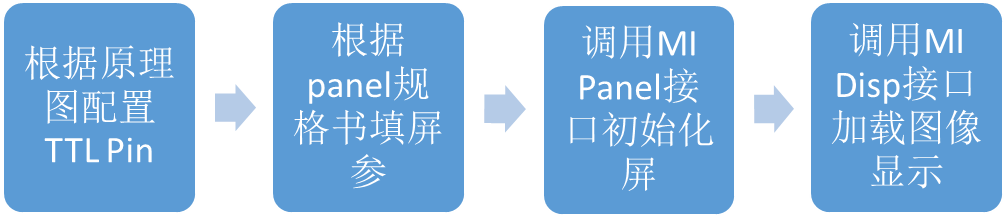
2.3. Panel Lighting Flow
2.4. Hardware related
2.4.1. View schematic
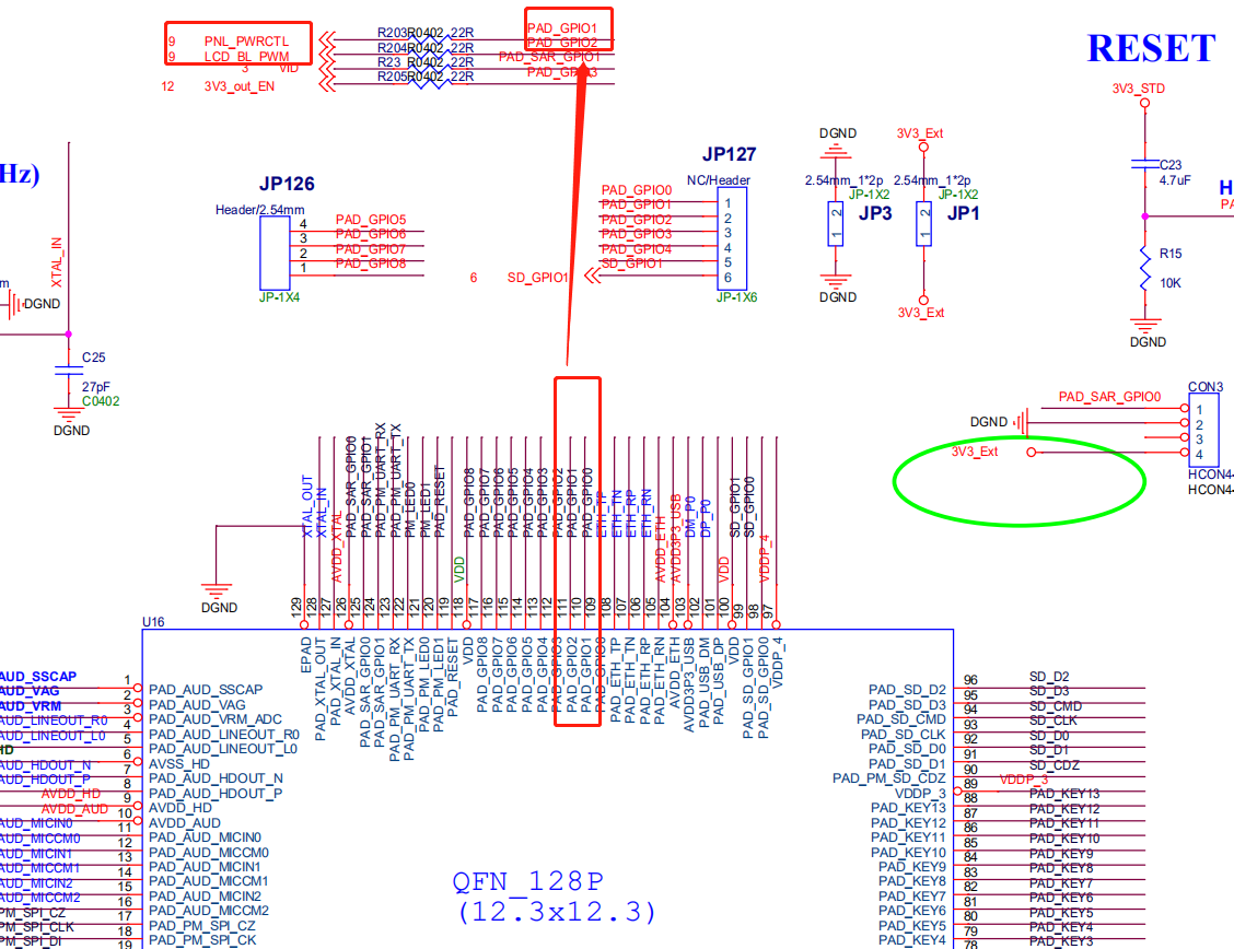
Take the schematic diagram of SSD202 demo board as an example.
Check the following schematic diagram to know the RGB888 data format and the corresponding Pins of CLK/HSYNC/VSYNC/DE:
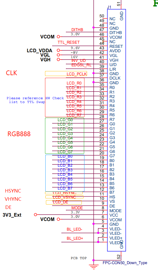
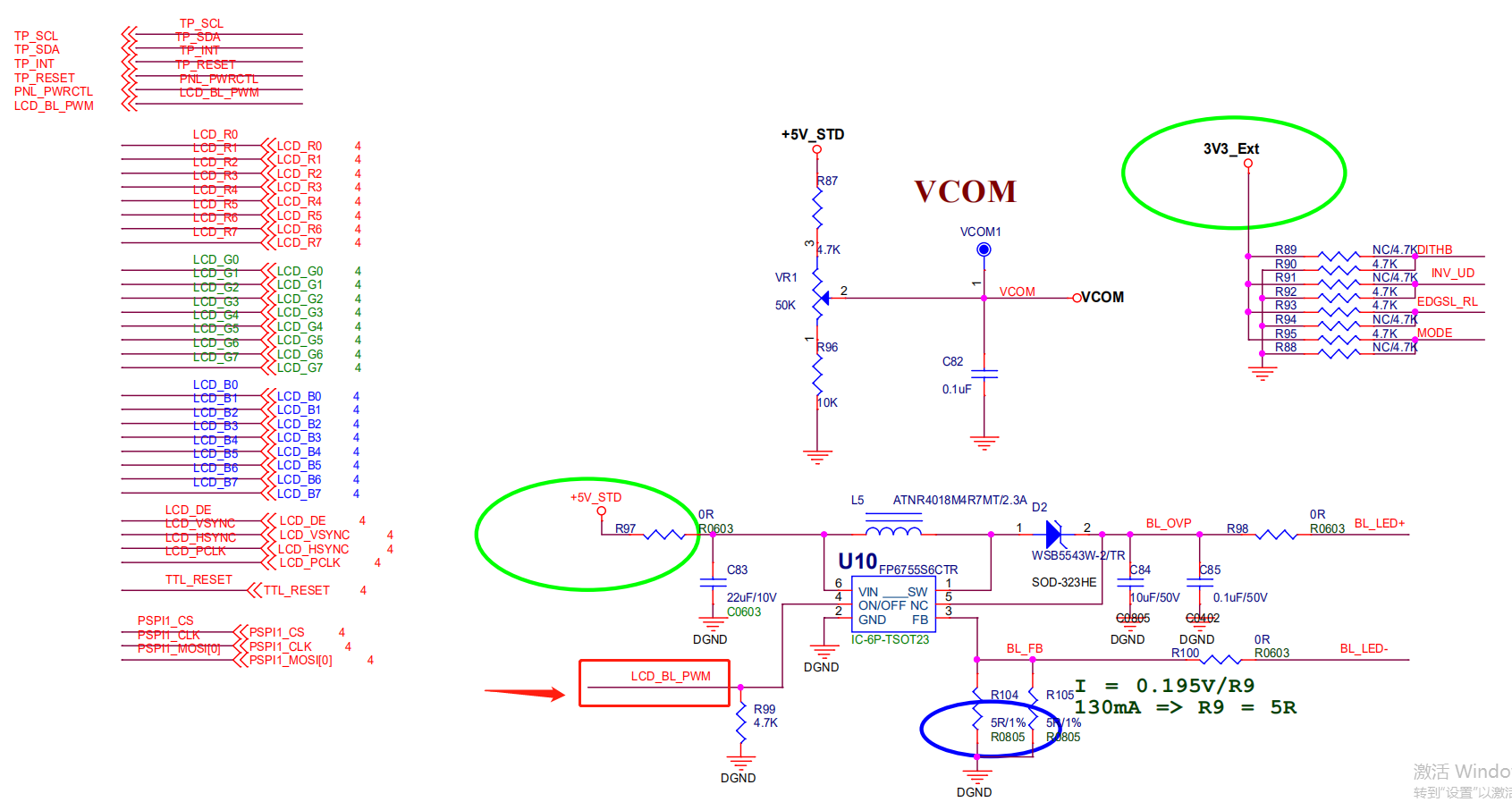
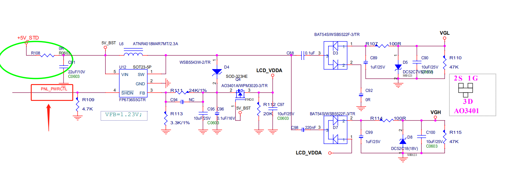
Check the following schematic diagram to know the PWM (LCD_BL_PWM) and panel power enable (PNL_PWRCTL) required to control the timing sequence:
The corresponding pins on the chip side are as follows:

The control sequence is as follows:
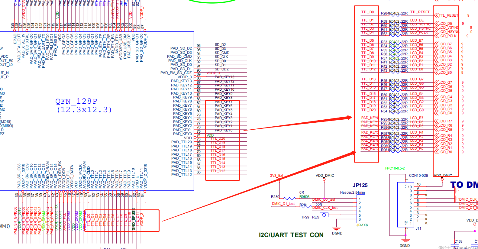
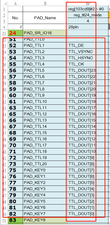
2.4.2. Corresponding to Padmux
Check the Tmux page of SSD222X HW CheckList V03.xlsx to find the padmux corresponding to the pin, as follows:
The signal pins are as follows:
The control pins are as follows:
2.5. Software related
2.5.1. Configuring padmux
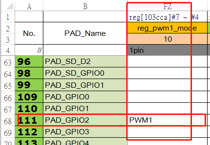
It can be seen from the above that the panel uses ttl24_mode_4, and pioneer3-ssc020a-s01a-demo-camera-padmux.dtsi corresponding to the kernel (the corresponding padmux.dtsi is different if the config used is different) is configured as follows:
2.5.2. Configure control pins (pwm/power)
This part is written in the project/board/ini/misc/config.ini of the Panel parameter configuration. If the related control in the Panel parameter is not used, the pwm pin needs to be configured as pwm mode in the padmux, and the enable power pin is configured as Corresponds to GPIO. The corresponding fields and meanings in the Panel parameters are as follows:
| m_ePanelPwBlCtrl = 1; | Indicates whether to control the timing of pwm and power in config. 0: Disable the following configuration. 1: Enable the following configuration. |
|---|---|
| m_wPanelPwGpioNum = 62; | sw index corresponding to Power gpio. |
| m_wPanelPwmNum = 1;#pwm num not gpio index!!! | Pwm number, meaning pwm0/pwm1/pwm2. pwm num is not gpio index. |
| m_wPanelDutyVal = 200000; | Pwm duty. |
| m_wPanelDlyTm2Data = 0; | Delay time between Power and data. |
| m_wPanelDlyTmData2Bl = 100; | Delay time between backlight and data. |
| m_wPanelPeriodVal = 200000; | Pwm Period . |
2.5.3. Panel parameter configuration
-
Panel parameter configuration file introduction
The path of the Panel parameter configuration file in alkaid is project/board/ini/misc/config.ini. During the system startup process, the Panel parameter configuration file will be parsed, and then different Panel parameters will be saved to the system for use by the display module. The display module will obtain the required Panel parameters from the system according to the parameters set by the user to call the API.
The Panel parameter configuration file consists of section and variable name:
-
section :
Fields in "[]" in the file.
-
variable name:
The field on the left of "=" in the file, and the value assigned to the variable name on the right
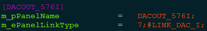
Sections are unique and are not allowed to have the same name, but variable names are allowed. As shown above, there can only be one section DACOUT_576I, but m_pPanelName can be in different sections. The system distinguishes variable names according to different sections, and then adds different Panel parameters.
The field of variable name is pre-defined by the system. When adding a new Panel parameter, you can only fill in the existing one in the system. Please inform the owner when adding or modifying it, otherwise the system will not recognize it. For example, m_pPanelName can only use m_pPanelName to define a new panel name when adding Panel parameters.
An example of variable name assignment is as follows:
-
-
Add Panel parameters
-
The new Panel parameter definition section name cannot be the same as the existing section name;
-
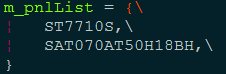
Add the section name of the new Panel parameter to the m_pnlList variable of the ROOT section (only one LCD section of different interfaces can exist, for example, there is already a TTL panel section name in m_pnlList, then if you want to add a new TTL, you can only delete the existing section);
-
Add new Panel parameters to the new section, as follows:

-
-
Panel parameter description
Parameter Description m_pPanelName panel name m_bPanelDither 1:enable Dither 0:disable Dither m_ePanelLinkType Interface type TTL :0 MIPI_DSI :10 m_bPanelInvDCLK Pixel clk polarity inversion m_bPanelInvDE DE polarity inversion m_bPanelInvHSync Hsync polarity inversion m_bPanelInvVSync Vsync polarity inversion m_wPanelHSyncWidth Pulse width of horizontal sync signal m_wPanelHSyncBackPorch HSync Back Porch m_wPanelVSyncWidth VSync signal pulse width m_wPanelVBackPorch VBackPorch m_wPanelHStart m_wPanelHSyncWidth+m_wPanelHSyncBackPorch m_wPanelVStart m_wPanelVSyncWidth+ m_wPanelVBackPorch m_wPanelWidth Number of valid pixels in a row m_wPanelHeight field valid number of lines m_wPanelHTotal m_wPanelWidth+m_wPanelHSyncWidth+m_wPanelHSyncBackPorch+HsyncFrontPorch m_wPanelVTotal m_wPanelHeight+m_wPanelVSyncWidth+ m_wPanelVBackPorch+VsyncFrontPorch m_wPanelDCLK m_wPanelHTotal m_wPanelVTotal fps (IP uses clk internally) m_wSpreadSpectrumFreq Clock spread amplitude modulation (see Spread Spectrum Calculation v2.xlsx) m_wSpreadSpectrumRatio Clock spread frequency modulation (see Spread Spectrum v2.xlsx) m_eOutputFormatBitMode 0: 10BIT; 1: 6BIT; 2: 8BIT; 3: 565BIT m_wPadmux TTL mode in Padmux m_ucPanelSwapChnR Swap Channel R. 0: default; 1: select R; 2: select G; 3: select B m_ucPanelSwapChnG Swap Channel G. 0: default; 1: select R; 2: select G; 3: select B m_ucPanelSwapChnB Swap Channel B. 0: default; 1: select R; 2: select G; 3: select B m_ucPanelSwapRgbML Swap Rgb MSB/LSB. 0: disable M/L swap; 1: enable M/L swap If it is a mipi panel, you also need to configure the mipi dsi:
MIPI DSI parameter description:
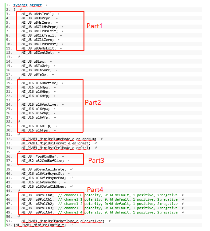
Parameters Description m_wHsTrail Default: 5 m_wHsPrpr Default: 3 m_wHsZero Default: 5 m_wClkHsPrpr Default: 10 m_wClkHsExit Default: 14 m_wClkTrail Default: 3 m_wClkZero Default: 12 m_wClkHsPost Default: 10 m_wDaHsExit Default: 5 m_wContDet Default:0 m_wLpx Default:16 m_wTaGet Default:26 m_wTaSure Default:24 m_wTaGo Default:50 m_wHactive Follow Panel parameter setting m_wHpw Follow Panel parameter setting m_wHbp Follow Panel parameter setting m_wHfp Follow Panel parameter setting m_wVactive Follow Panel parameter setting m_wVpw Follow Panel parameter setting m_wVbp Follow Panel parameter setting m_wVfp Follow Panel parameter setting m_wBllp 0 m_wFps Default:60 m_eLaneNum one lane :1 two lane :2 three lane :3 four lane :4 m_eFormat RGB565 :0 RGB666 :1 LOOSELY_RGB666 :2 RGB888 :3 m_eCtrlMode CMD_MODE :0 SYNC_PULSE :1 SYNC_EVENT :2 BURST_MODE :3 m_ucClkLane Clk lane selection(default:2) 0:select chn0 1:select chn1 2:select chn2 3:select chn3 4:select chn4 m_ucDataLane0 data lane0 selection(default:4) 0:select chn0 1:select chn1 2:select chn2 3:select chn3 4:select chn4 m_ucDataLane1 data lane1 selection(default:3) 0:select chn0 1:select chn1 2:select chn2 3:select chn3 4:select chn4 m_ucDataLane2 data lane2 selection(default:1) 0:select chn0 1:select chn1 2:select chn2 3:select chn3 4:select chn4 m_ucDataLane3 data lane3 selection(default:0) 0:select chn0 1:select chn1 2:select chn2 3:select chn3 4:select chn4 m_pCmdBuff Mipi panel cmd m_pCmdBuff= m_ucPolCh0 Chn0极性 0:default 1:positive 2:negative m_ucPolCh1 Chn1极性 0:default 1:positive 2:negative m_ucPolCh2 Chn2 polarity 0: default 1: positive 2: negative m_ucPolCh3 Chn3 polarity 0: default 1: positive 2: negative m_ucPolCh4 Chn4 polarity 0: default 1: positive 2: negative -
Fill in the Panel parameters according to the specification
Find the following table according to the specification of the Panel:
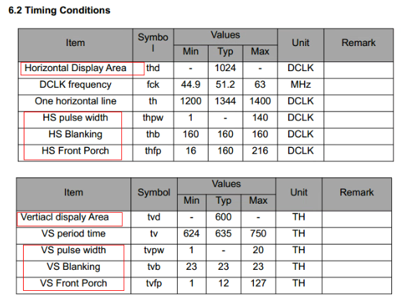
HTotal = u16Width + u16HSyncWidth + u16HSyncBackPorch + HSyncFrontPorch

VTotal = u16Heigth + u16VSyncWidth + u16VSyncBackPorch + HVyncFrontPorch

DCLK = HTotal * VTotal * FPS
You need to fill in the following according to the Panel specification:
m_wPanelHSyncWidth

m_wPanelHSyncBackPorch

m_wPanelVSyncWidth

m_wPanelVBackPorch

m_wPanelHStart

m_wPanelVStart

m_wPanelWidth

m_wPanelHeight

m_wPanelHTotal

m_wPanelVTotal

m_wPanelDCLK
The following is the relevant data filled in the public version:

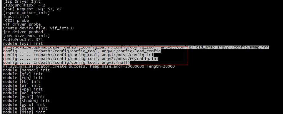
The parsing of config.ini is automatically loaded into mi_sys through config_tool when insmode is turned on, and mi_disp and mi_panel only need to be used directly, and no manual loading is required.
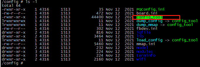
The default load path of config.ini is:
First priority path: /misc/config.ini
Second priority path: /config/config.ini
Third priority path: /config/model/config.ini
2.5.4. Code Examples
SSD2X2 and SSD20X differ in the way of loading Panel parameters. SSD20X saves the Panel parameters in a header file, and reads the relevant parameters from the header file through the MI_PANEL_SetPanelParam function during initialization. SSD2X2 saves the Panel parameters in the project/board/ini/misc/config.ini file, sets the corresponding interface type by calling the MI_PANEL_Init function, parses the config.ini file and loads the corresponding Panel parameters.
MI_PANEL_IntfType_e eIntfType;

eIntfType = E_MI_PNL_INTF_TTL; //TTL interface

MI_PANEL_Init(eIntfType);
2.6. Debug method
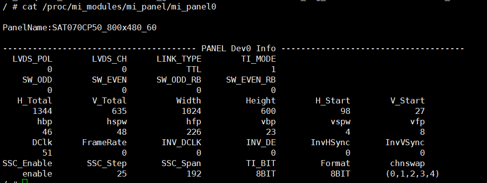
2.6.1. Cat the module node corresponds to the system
cat /proc/mi_modules/mi_panel/mi_panel0
2.6.2. Common debug registers
After calling the MI_DISP related API to initialize the display device, you can write the register through riu_w 1128 7 a, type the test pattern to PANEL, and verify whether the PANEL Panel parameters are configured successfully.
3. MIPI Panel introduction
3.1. Specifications
| Specification Chip |
MIPI |
|---|---|
| 201/201 | Support |
| 21X/22X | Not supported |
| 203 | Not supported |
MIPI DSI Specifications:
-
1-4 data lanes, 1 clock lane
-
Level
LP: 0~12V
HS: 100~300mV
-
HS: 80Mbps ~ 1.5Gbps/lane
-
Pixel format
16 bpp (5,6,5 RGB) each pixel using two bytes
18 bpp (6,6,6 RGB) packed
18 bpp (6, 6, 6 RGB) loosely packed into three bytes
24 bpp (8, 8, 8 RGB), each pixel using three bytes
-
video mode: BURST_MODE/SYNC_EVENT/SYNC_PULSE
-
data/clk chn swap
-
data/clk chn P/N swap
-
data clk skew adjustment
3.2. Basic Concepts
MIPI DPHY timing chart:
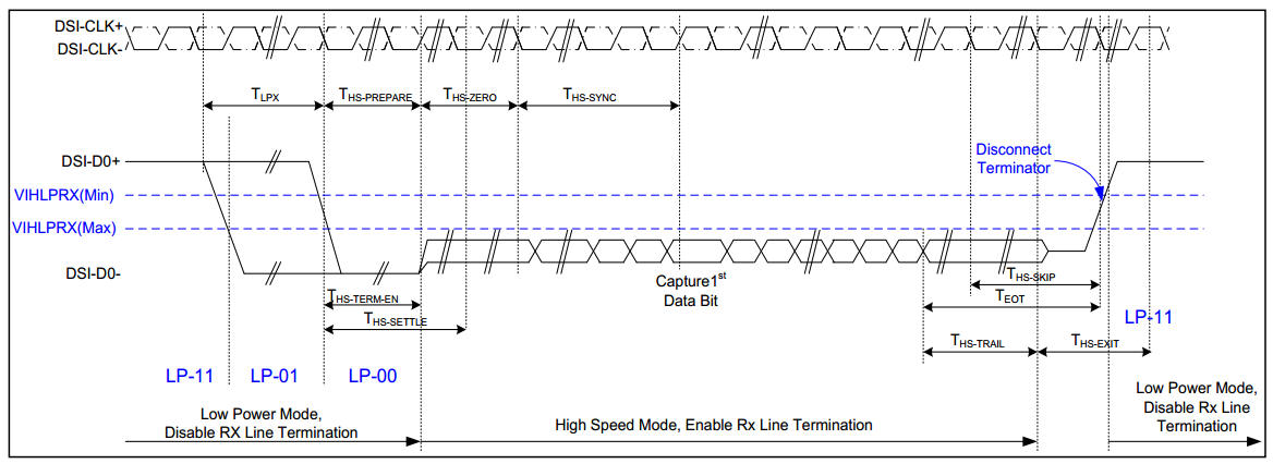
Figure3-1 Data lanes-Low Power Mode to/from High Speed Mode Timing

Figure3-2 Clock lanes- High Speed Mode to/from Low Power Mode Timing
-
Configure HS Timing Parameter
HS_TRAIL/HS_EXIT /HS_PRPR/HS_ZERO/CLK_PRPR/CLK_ZERO/CLK_POST/CLK_TRAIL
Timing specification THS-PREPARE + THS-zero 145ns+10 * UI THS-PREPARE 40ns+4 * UI ~ 85ns +6 * UI THS-ZERO >60ns+4 * UI ~105ns+6 * UI UI represents the time interval, equal to the duration of any HS state on the clock channel.
UI calculation method:
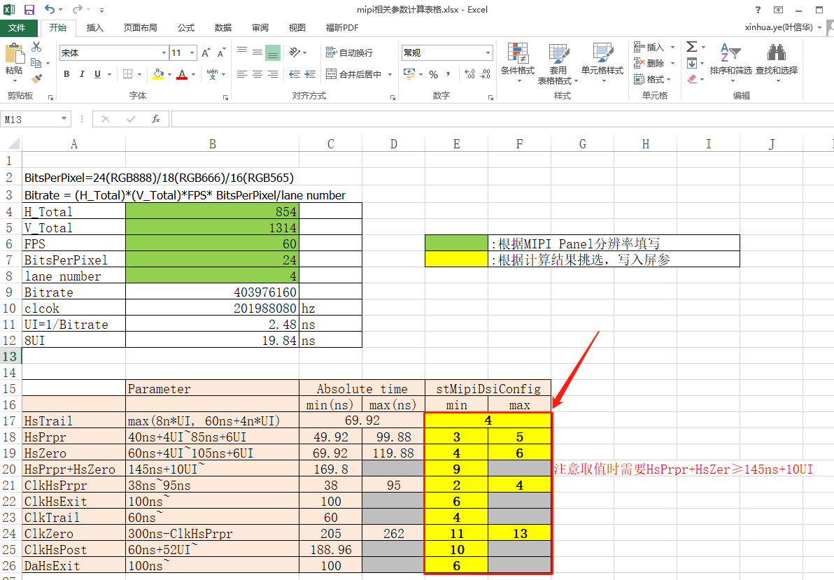
H_Total = HACT+HPW+HBP+HFP

V_Total = VACT+VPW+VBP+VFP

BitsPerPixel=24(RGB888)/18(RGB666)/16(RGB565)

Bitrate = (H_Total)*(V_Total)*FPS* BitsPerPixel/lane number

UI = 1/Bitrate
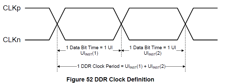
Figure 3-3 DSI clock channel timing
If Bitrate = 750Mps, UI = 1/Bitrate = 1.333ns, then the calculation result of HS timing parameter is:
Timing specification Absolute time DA_HS_PREP value (Absolute time/(8*UI)) THS-PREPARE + THS-zero 145ns+10*UI > 158.33 ns > 15 THS-PREPARE 40ns+4 * UI ~ 85ns +6 * UI 45.32 ~ 92.98 ns 5 ~ 8 THS-zero >60ns+4 * UI ~105ns+6 * UI > 112.98~ 65.32 ns 10 ~ 7 -
Configure LP Timing Parameter
CONT_DET/LPX/TA_GET/TA_SURE/TA_GO
It is recommended to use the provided default values for low power parameters
DCS (Display Command Set) protocol: DCS is a standardized command set for display modules in command mode.
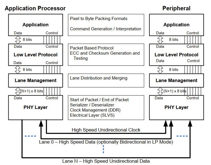
DSI (Display Serial Interface) is divided into four layers, corresponding to D-PHY, DSI, DCS specifications, and the layered structure diagram is as above:
-
PHY: The transmission medium, input/output circuits and clocking and signaling mechanisms.
-
Lane Management layer: Send and collect data flow to each lane.
-
Low Level Protocol layer: How to frame and parse, and error detection.
-
Application layer: High-level encoding and parsing data streams.
-
3.3. Hardware related
3.3.1. View schematic
Demo Board schematic:
As shown in the figure above, the corresponding pins inside the chip by default are:
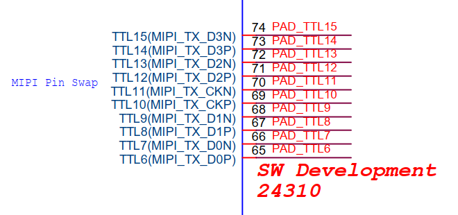
Lane0 corresponds to PAD_TTL6/7 → E_MI_PNL_CH_SWAP_0 (the corresponding enumeration value is 0)
Lane1 corresponds to PAD_TTL8/9 → E_MI_PNL_CH_SWAP_1 (the corresponding enumeration value is 1)
Lane2 corresponds to PAD_TTL12/13 → E_MI_PNL_CH_SWAP_3 (the corresponding enumeration value is 3)
Lane3 corresponds to PAD_TTL14/15 → E_MI_PNL_CH_SWAP_4 (the corresponding enumeration value is 4)
Clk corresponds to PAD_TTL10/11 → E_MI_PNL_CH_SWAP_2 (the corresponding enumeration value is 2)
The enumeration values here are software-defined, refer to the MIPI Swap field configuration described next.
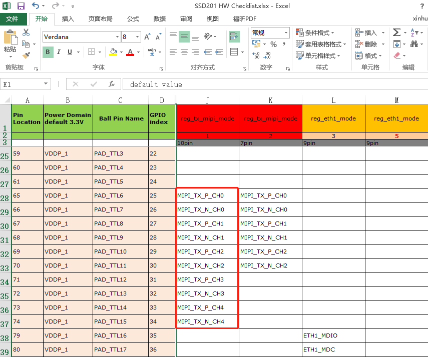
3.3.2. Corresponding to padmux
Confirm the hardware design pin connection
The following picture is the recommended mipi pin, PAD TTL6 – PAD TTL15 (MIPI Mode 1)
3.4. Software related
3.4.1. Configuring padmux
-
User space configuration Find the *padmux.dts configuration corresponding to the project corresponding to MIPI MODE
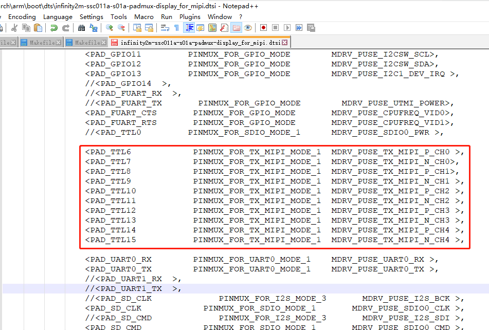
-
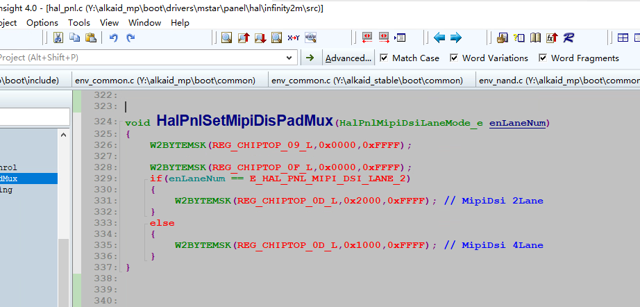
Padmux configuration under Uboot
MIPI is commonly used 2Lane and 4Lane. Under Uboot, it has been automatically switched to the corresponding Mode according to the Lane num of the Panel parameter. Users can use it directly without paying attention.
3.4.2. Configure Panel parameters
Confirm panel specifications:

HTotal = u16Width + u16HSyncWidth + u16HSyncBackPorch + HSyncFrontPorch

VTotal = u16Heigth + u16VSyncWidth + u16VSyncBackPorch + HVyncFrontPorch

DCLK = HTotal * VTotal * FPS
3.4.3. Code Examples
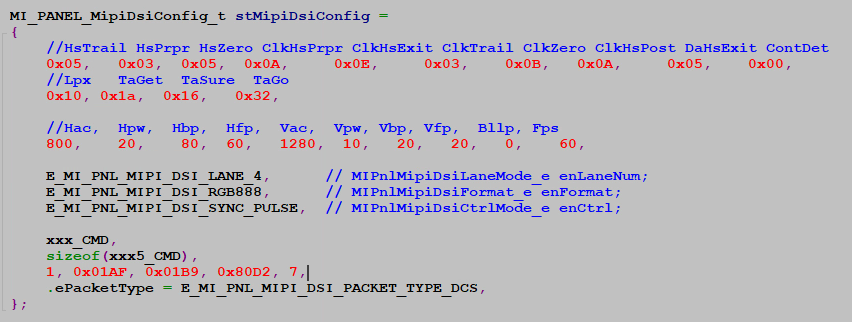
MIPI Panel parameters will be slightly different than that of TTL, mainly focus on two structures, pay attention to the parameter settings:
-
Configure MI_PANEL_MipiDsiConfig_t (TTL does not need to be concerned)
-
Part 2 is mainly to set the H/V related parameters listed in the Panel specification, and fill in the connection options one by one according to the TTL method.
-
Part3 is mainly the initialization cmd of the Panel. This part of the cmd is customized by each panel manufacturer with reference to the DSC standard, so the cmd is generally provided by the original chip manufacturer of the Panel.
1. static MI_U8 cmd_buf[] = 2. { 3. cmd1, data_num, data[0],data[1],...,data[num-1], 4. ..., 5. cmdN, data_num, data[0],data[1],...,data[num-1], 6. FLAG_END_OF_TABLE, FLAG_END_OF_TABLE, //Terminator 7. } -
Part4 is to set the P/N polarity of each Lane to be reversed. Refer to the connection between the hardware and the Panel to confirm whether it needs to be reversed.
-
Part 1 is mainly for the timing requirements during the transmission process. In this part, we have prepared a general Excel table (mipi related parameter calculation v2.xlsx). As long as you input the HTotal/VTotal corresponding to the Panel, it will be automatically generated. The example is as follows:
The red box part is the scream that is automatically generated according to the formula, and you can fine-tune the corresponding and fill in the software Panel parameters within the range.
-
-
MI_PANEL_ParamConfig_t: mainly depends on the MIPI Swap configuration field (TTL does not need to be concerned)
1.    typedef enum
2.    {
3.        E_MI_PNL_CH_SWAP_0,
4.        E_MI_PNL_CH_SWAP_1,
5.        E_MI_PNL_CH_SWAP_2,
6.        E_MI_PNL_CH_SWAP_3,
7.        E_MI_PNL_CH_SWAP_4,
8.    }MI_PANEL_ChannelSwapType_e;
9.
10.    typedef struct
11.    {
12.        ...
13.        ...
14.        MI_PANEL_ChannelSwapType_e eCh0;   //--> CLK  field
15.        MI_PANEL_ChannelSwapType_e eCh1;   //--> Lane3 field
16.        MI_PANEL_ChannelSwapType_e eCh2;   //--> Lane2 field
17.        MI_PANEL_ChannelSwapType_e eCh3;   //--> Lane1 field
18.        MI_PANEL_ChannelSwapType_e eCh4;   //--> Lane0 field
19.    }MI_PANEL_ParamConfig_t;
You need to refer to the actual hardware connection configuration. Considering that the external device Lane To Lane does not do Swap, the parameters should be configured as follows:
1.    typedef struct
2.    {
3.        ...
4.        ...
5.        MI_PANEL_ChannelSwapType_e eCh0;   //--> CLK field        -- E_MI_PNL_CH_SWAP_2
6.        MI_PANEL_ChannelSwapType_e eCh1;   //--> Lane3 field       -- E_MI_PNL_CH_SWAP_4
7.        MI_PANEL_ChannelSwapType_e eCh2;   //--> Lane2 field       -- E_MI_PNL_CH_SWAP_3
8.        MI_PANEL_ChannelSwapType_e eCh3;   //--> Lane1 field       -- E_MI_PNL_CH_SWAP_1
9.        MI_PANEL_ChannelSwapType_e eCh4;   //--> Lane0 field       -- E_MI_PNL_CH_SWAP_0
10.    }MI_PANEL_ParamConfig_t;
That is 2, 4, 3, 1, 0
Panel parameter example:
1.    int sstar_disp_init(MI_DISP_PubAttr_t *pstDispPubAttr, int disp_port_num)
2.    {
3.        MI_PANEL_LinkType_e eLinkType;
4.
5.        if (pstDispPubAttr->eIntfType == E_MI_DISP_INTF_LCD)
6.        {
7.            pstDispPubAttr->stSyncInfo.u16Vact = stPanelParam.u16Height;
8.            pstDispPubAttr->stSyncInfo.u16Vbb = stPanelParam.u16VSyncBackPorch;
9.            pstDispPubAttr->stSyncInfo.u16Vfb = stPanelParam.u16VTotal - (stPanelParam.u16VSyncWidth +
10.                                                                          stPanelParam.u16Height + stPanelParam.u16VSyncBackPorch);
11.            pstDispPubAttr->stSyncInfo.u16Hact = stPanelParam.u16Width;
12.            pstDispPubAttr->stSyncInfo.u16Hbb = stPanelParam.u16HSyncBackPorch;
13.            pstDispPubAttr->stSyncInfo.u16Hfb = stPanelParam.u16HTotal - (stPanelParam.u16HSyncWidth +
14.                                                                          stPanelParam.u16Width + stPanelParam.u16HSyncBackPorch);
15.            pstDispPubAttr->stSyncInfo.u16Bvact = 0;
16.            pstDispPubAttr->stSyncInfo.u16Bvbb = 0;
17.            pstDispPubAttr->stSyncInfo.u16Bvfb = 0;
18.            pstDispPubAttr->stSyncInfo.u16Hpw = stPanelParam.u16HSyncWidth;
19.            pstDispPubAttr->stSyncInfo.u16Vpw = stPanelParam.u16VSyncWidth;
20.            pstDispPubAttr->stSyncInfo.u32FrameRate = stPanelParam.u16DCLK * 1000000 / (stPanelParam.u16HTotal * stPanelParam.u16VTotal);
21.            pstDispPubAttr->eIntfSync = E_MI_DISP_OUTPUT_USER;
22.            pstDispPubAttr->eIntfType = E_MI_DISP_INTF_LCD;
23.            eLinkType = stPanelParam.eLinkType;
24.
25.            MI_DISP_SetPubAttr(0, pstDispPubAttr);
26.            MI_DISP_Enable(0);
27.
28.            MI_PANEL_Init(eLinkType);
29.            MI_PANEL_SetPanelParam(&stPanelParam);
30.            if(eLinkType == E_MI_PNL_LINK_MIPI_DSI)
31.            {
32.                MI_PANEL_SetMipiDsiConfig(&stMipiDsiConfig);
33.            }
34.
35.        }
36.        return 0;
3.5. Debug method
cat /proc/mi_modules/mi_panel/mi_panel0
4. Other types of panel lighting
4.1. SPI panel lighting
4.1.1. Specifications
| Specification Chip |
SPI |
|---|---|
| 201/202 | Support |
| 21X/22X | Support |
| 203 | Support |
4.1.2. Basic Concepts
SPI: Serial Peripheral Interface.
Use the spi interface to generally point to a smaller resolution lcd.
4.1.3. Panel Lighting Flow
Step 1:
Configure the SPI PIN according to the schematic diagram. Query the CheckList table and change the dts file to configure the PIN_MUX of the corresponding pin.
Step 2:
Enable SPI driver in Kernel
Enable the following options under menuconfig:
> Device Drivers

    >Sstar Soc platform drivers

        >Sstar MSPI driver
Step 3:
According to the data sheet under the initialization command. The initialization command is generally provided by the panel factory, or you can view the panel specification and configure it yourself.
Step 4:
Write image data and display the Panel. Some Panels come with an internal test part, which can be enabled for output through commands.
4.1.4 Hardware related
4.1.4.1 View schematic
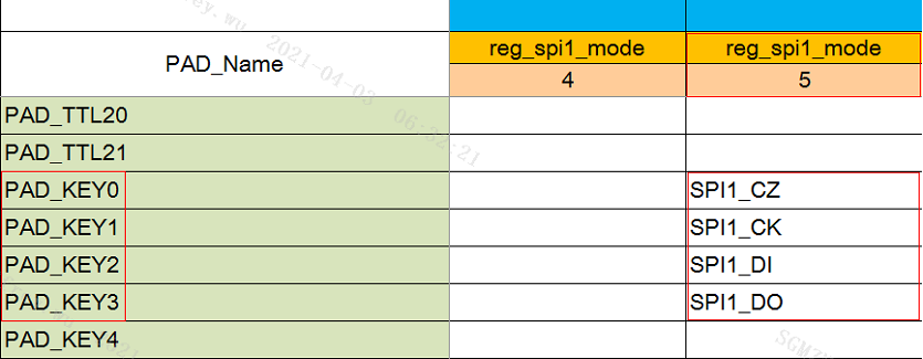
Taking SPI as an example, a hardware engineer will query the HW CheckList table when drawing a schematic diagram, and select a set of free pins that can be used as SPI interface pins. We choose PAD_KEY0~3 to be multiplexed as SPI1, and PADMUX choose SPI1_MODE_5.
4.1.4.2 for padmux
4.1.5 Software related
4.1.5.1 Configure related padmux
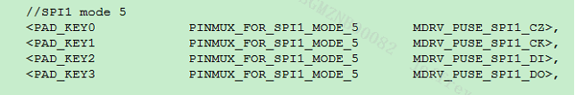
In the case of PADMUX with known pins, we need to change the padmux.dtsi file in the kernel/arch/arm/boot/dts directory to ensure that the PADMUX is switched correctly. Take SPI1_MODE_5 as an example:
In the kernel/drivers/sstar/gpio/pioneer3/mhal_pinmux.c file, you can find the PADMUX that can be configured for each pin, as well as the related registers. We can confirm whether the PADMUX is switched correctly by reading the value of the register through the riu tool on the board side. Take the SSD2X2 platform as an example:
1. #define PADTOP_BANK 0x103C00 //Base address

2. #define REG_SPI1_MODE 0x68 //Offset address

3. #define REG_SPI1_MODE_MASK BIT8|BIT9|BIT10|BIT11 //valid bit
riu_r 103C 68, if the read value is 0x500, it indicates that the PADMUX switch is correct.
4.1.5.2 Configure Panel parameters
SPI does not have the Panel parameter configuration similar to our TTL, mainly according to the initialization command under the data sheet. The initialization command is generally provided by the panel factory, or you can view the panel specification and configure it yourself.
4.1.5.3 Code Examples
smartdisp_demo\P3_ReleaseDemo\panel\SpiPanel
Note that there are two methods of spi implementation in this demo: hardware spi and gpio simulation. It is recommended to use the hardware spi method inside our chip.
4.1.6. Development Recommendations
It is recommended to use the native architecture of the kernel to develop with the spi panel, you can refer to:
4.1.7 Debug method
If the SPI Panel does not light up, you can check it from the following methods:
-
Is the padmux of spi configured correctly? It can be confirmed by looking at the registers and measuring the waveform in hardware.
-
Whether the spi initialization command is correct, you can contact the Panel factory to confirm, and you can send the command through spi to play the test pattern to test whether the hardware is connected.
4.2. PSPI panel lighting
4.2.1 Specifications
| Specification Chip |
PSPI |
|---|---|
| 201/202 | Not supported |
| 21X/22X | Support |
| 203 | Not supported |
4.2.2 Basic Concepts
The PSPI module is a private SPI protocol newly added to the SSD2X2 platform, supports Master/Slave mode, and has a maximum clock of 216MHz. When the Panel is clicked, it is configured as Master mode, and the PANEL is required to support TE Mode.
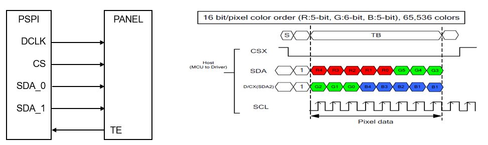
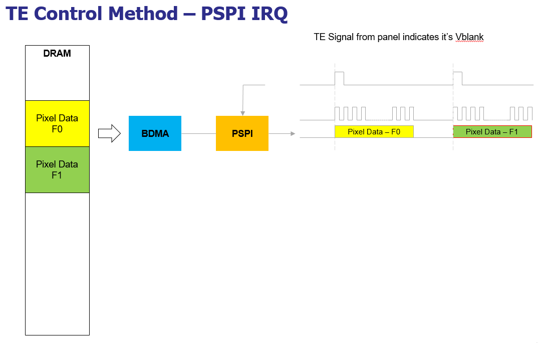
The PSPI module supports two-wire mode, that is, one clock transmits two bits. When configured in two-wire mode, the maximum configuration of PSPI's DCLK is 108MHz. The TE signal is a control signal for synchronization, that is, the refresh rate of the Panel. The PSPI module will send a field of data to the PANEL after receiving the rising edge of the TE signal. DCLK needs to satisfy DCLK>hTotal * vTotal * Pixel * FPS / 2, to ensure that PSPI transmits one field of data within the interval of the TE signal.
The working mode of TE Mode is shown in the following figure:
4.2.3 Hardware related
4.2.3.1 Configuration pin PADMUX
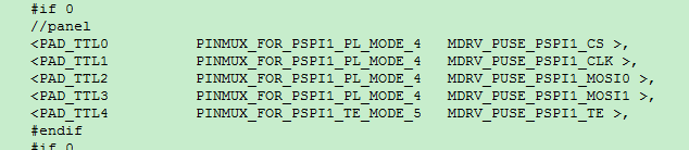
Query the HW Checklist table to find the multiplexing mode corresponding to the pin. In the following example, configure PAD_TTL0~PAD_TTL3 as PSPI1_PL_MODE_4, and configure PAD_TTL4 as PSPI1_TE_MODE_5.

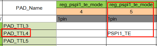
Modify the padmux.dtsi device tree file under kernel/arch/arm/boot/dts and configure the PADMUX of the corresponding pin.
Taking the SSD2X2 platform as an example, the relevant registers are defined in the kernel/drivers/sstar/gpio/pioneer3/mhal_pinmux.c file. By reading the value of the register, you can confirm whether the PADMUX switch is OK.
riu_r 103C 6A, if the read value is 0x504, the PADMUX switch is correct.
4.2.4 Software related
4.2.4.1 Panel initialization
After the PADMUX configuration of the pins is completed, an initialization command needs to be sent to the Panel. The initialization command is generally provided by the panel factory or configured by the user by referring to the panel specification. When the PSPI module is configured in single-wire mode, it is equivalent to an SPI peripheral, and can call the relevant API to send commands.
Call the MI_PSPI_Transfer interface to send the initialization command to the panel.
1. MI_PSPI_Msg_t pspi_msg;
2. MI_PSPI_Param_t pspi_para;
3. MI_PSPI_DEV pspi_dev = 1;//Select 1 when using PSPI to point the Panel dev
4.
5. pspi_para.u8BitsPerWord = 9;//Data length, common 8bit/9bit, maximum 16bit
6. pspi_para.u8DataLane = DATA_SINGLE;//Single line mode
7. pspi_para.u16DelayCycle = 2;
8. pspi_para.u16WaitCycle = 2;
9. pspi_para.u8RgbSwap = 0;
10. pspi_para.u32MaxSpeedHz = 1000000;//PSPI clock frequency, single line mode up to 216MHz
11. pspi_para.u16PspiMode = 0;
12. pspi_para.u8ChipSelect = MI_PSPI_SELECT_0;
13. pspi_para.u8TeMode = 0;// Turn off TE MODE first when sending commands as normal SPI
14. MI_PSPI_CreateDevice(pspi_dev, &pspi_para);//
15.
16. memset(&pspi_msg, 0 ,sizeof(MI_PSPI_Msg_t));
17. pspi_msg.u8TxBitCount = 9;
18. pspi_msg.u8TxSize = 8;//Transfer a maximum of 8 data at a time
19. pspi_msg.au16TxBuf[0] = 0xDA; //command
20. pspi_msg.au16TxBuf[1] = 0x1FF;//data
21. pspi_msg.au16TxBuf[2] = 0x1AB;
22. pspi_msg.au16TxBuf[3] = 0x104;
23. pspi_msg.au16TxBuf[4] = 0x1D2;
24. pspi_msg.au16TxBuf[5] = 0x108;
25. pspi_msg.au16TxBuf[6] = 0x1C2;
26. pspi_msg.au16TxBuf[7] = 0x133;
27. MI_PSPI_Transfer(pspi_dev, & pspi_msg);
4.2.4.2 Display Test
The user layer needs to call the API related to MI SYS and PSPI, and fill in the RGB data into the PSPI module. After the PSPI module receives the TE signal fed back by the PANEL, it will send the image data to the PANEL for display. The specific code implementation can refer to the following.
1. MI_PSPI_Msg_t pspi_msg;
2. MI_PSPI_Param_t pspi_para;
3. MI_PSPI_DEV pspi_dev = 1;//Select 1 when using PSPI to point the Panel dev
4.
5. pspi_para.u8TeMode = 1;//Open TE MODE
6. pspi_para.u32MaxSpeedHz = 24 * 1000 * 1000;//Configure the clock
7. pspi_para.u8DataLane = DATA_DUAL;//Dual line mode
8.  MI_PSPI_SetDevAttr(pspi_dev, &pspi_para);
9.
10. MI_SYS_ChnPort_t  stChnPort;
11. MI_SYS_BufConf_t  stBufConf;
12. MI_SYS_BUF_HANDLE stHandle;
13. MI_SYS_BufInfo_t  stBufInfo;
14. memset(&stChnPort, 0, sizeof(MI_SYS_ChnPort_t));
15. memset(&stBufConf, 0, sizeof(MI_SYS_BufConf_t));
16. memset(&stBufInfo, 0, sizeof(MI_SYS_BufInfo_t));
17. memset(&stHandle, 0, sizeof(MI_SYS_BUF_HANDLE));
18.
19. stChnPort.eModId    = E_MI_MODULE_ID_PSPI;//选中PSPI模块
20. stChnPort.u32DevId  = 1;
21. stChnPort.u32ChnId = 0;
22. stChnPort.u32PortId = 0;
twenty three.
24. stBufConf.eBufType = E_MI_SYS_BUFDATA_FRAME;
25. stBufConf.stFrameCfg.u16Height = IMAGE_HEIGHT;//The height of the image
26. stBufConf.stFrameCfg.u16Width = IMAGE_WIDTH;// The width of the image
27. stBufConf.stFrameCfg.eFrameScanMode = E_MI_SYS_FRAME_SCAN_MODE_PROGRESSIVE;
28. stBufConf.stFrameCfg.eFormat = E_MI_SYS_PIXEL_FRAME_RGB565;//The data format of the image
29.
30. //Apply for a buf to save image data,
31. if(MI_SYS_ChnInputPortGetBuf(&stChnPort, &stBufConf, &stBufInfo, &stHandle, -1) == MI_SUCCESS)
32. {
33.     //Copy the image data to the applied buf
34.     memcpy(stBufInfo.stFrameData.pVirAddr[0], TxBuf, stBufInfo.stFrameData.u32BufSize);
35.
36.     // Give the buf to the PSPI module for use. When the PSPI module receives the TE signal, it will send this image to the panel for display
37.     if(MI_SYS_ChnInputPortPutBuf(stHandle, &stBufInfo, FALSE) != MI_SUCCESS)
38.     {
39.         printf("MI_SYS_ChnInputPortPutBuf Failed!\n");
40.     }
41. }
4.2.5 Notes
-
When using the PSPI module to tap the PSPI device, only PSPI1 can be selected, that is, MI_PSPI_DEV=1
-
The maximum number of data transferred per MI_PSPI_Transfer is 8 by default.
-
The maximum clock of single-wire mode is 216MHz, and the maximum clock of dual-wire mode is 108Mhz.
4.3. SRGB panel lighting
4.3.1 Specifications
| Specification Chip |
SRGB |
|---|---|
| 201/202 | Not supported |
| 21X/22X | Support |
| 203 | Not supported |
4.3.2 Basic Concepts
SRGB is a serial RGB interface. Using this interface to transmit data, the RGB data of one pixel will be divided into three transmissions to the panel. As shown in the figure below, taking RGB888 as an example, for a TTL Panel, a DCLK clock can transmit 24-bit data, that is, a pixel, to the panel in parallel; for an SRGB interface Panel, a DCLK clock only transmits one byte. The transmission of R, G, and B data in a row requires 3 CLKs to transmit a pixel. Therefore, for a Panel with the same resolution, the clock frequency required by the SRGB interface is about three times higher than that of the TTL interface.
4.3.3 Hardware related
4.3.3.1 View schematic
4.3.2 for padmux
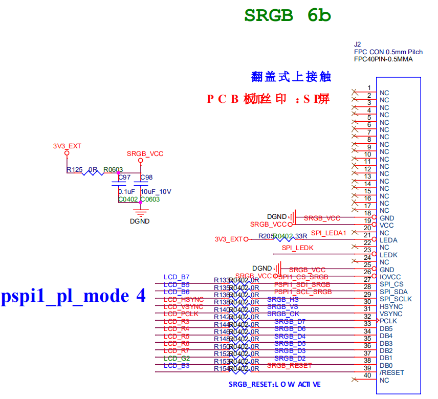
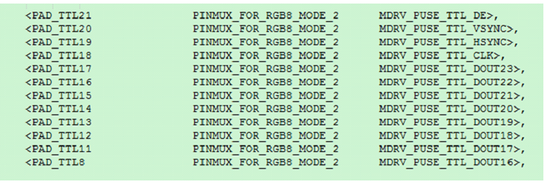
Check the HW Checklist table and make sure that the PAD_TTL8, PAD_TTL11~ PAD_TTL21 pins are selected as RGB8_MODE_2.

4.3.4 Software related
4.3.4.1 Configuring PADMUX
Modify the padmux.dtsi device tree file under kernel/arch/arm/boot/dts and configure the PADMUX of the corresponding pin.
Taking the SSD2X2 platform as an example, the relevant registers are defined in the kernel/drivers/sstar/gpio/pioneer3/mhal_pinmux.c file. By reading the value of the register, you can confirm whether the PADMUX switch is OK.
riu_r 103C 6B, if the read value is 0x2, the PADMUX switch is correct.
4.3.4.2 Fill in Panel parameters
The SRGB interface Panel is similar to the TTL Panel. It is also necessary to add the corresponding Panel parameters in config.ini according to the Panel specification, and then call MI_PANEL_Init to load the Panel parameters. Find several groups of parameters similar to the following in the Panel specification:

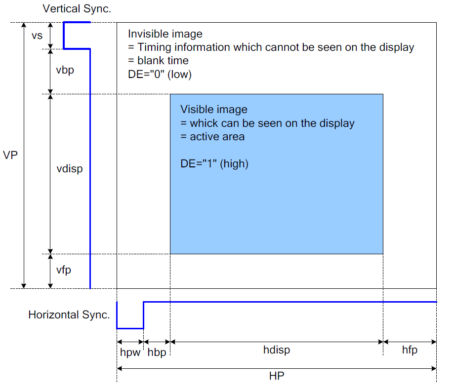
The relationship between the above parameters can be seen from the timing diagram:
V_Total = VS + VBP + VDISP + VFP
H_Total = HPW + HBP + HDISP + HFP
DCLK = H_Total * 3 * V_Total * FPS
Then fill in the parameters into config.ini, as shown in the following example:
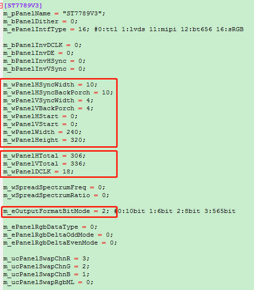
The values of HTotal, VTotal, and DCLK parameters can be calculated by the above formula. The effective display size of the Panel is 240x320, and the refresh rate is set to 60Hz, then:
m_wPanelHTotal= m_wPanelHSyncWidth+m_wPanelHSyncBackPorch+m_wPanelWidth+HFP=10+10+240+46=306

m_wPanelVTotal=m_wPanelVSyncWidth+m_wPanelVBackPorch+m_wPanelHeight+VFP=4+4+320+8=336

m_wPanelDCLK= m_wPanelHTotal*3*m_wPanelVTotal*FPS=306*3*336*60=18MHz
Because the SRGB interface is used, PADMUX is configured with RGB8 MODE, so m_eOutputFormatBitMode selects 2
4.3.4.3 Loading Panel parameters
The Panel parameter file is generally saved in the /misc directory on the board, and the user can also specify the path of the Panel parameter file with relevant parameters when insmod mi_sys.ko: insmod mi_sys.ko config_ini_path=“/misc/config.ini”
When the user layer calls the API related to MI PANEL, it will parse the ini file and load the corresponding Panel parameters.
1. MI_PANEL_IntfType_e eIntfType;

2. eIntfType = E_MI_PNL_INTF_SRGB; //Select SRGB interface

3.MI_PANEL_Init(eIntfType);
When filling in the Panel parameters, please note that there is only one Panel parameter of SRGB type under the m_pnlList field, otherwise the bottom layer of MI cannot correctly resolve the target Panel parameter.

4.3.4.4 Display Test
Use MI Test Parttern to test whether the SRGB Panel is initialized successfully.
riu_w 1128 7 A, if there are color bars on the Panel, it means the Panel is initialized successfully.
In addition, the RGB display dislocation problem can be corrected by adjusting the swap parameter in the ini.
1. m_ucPanelSwapChnR = 3;

2. m_ucPanelSwapChnG = 2;

3. m_ucPanelSwapChnB = 1;

4. m_ucPanelSwapRgbML = 0;
As above, the order of the RGB channels is 3, 2, 1. If the place where red is originally displayed is displayed as green, we can adjust the red and green channels by swapping, that is, change the order of RGB channels to 2, 3, and 1.
The color channel is confirmed by the following registers:
riu_w 1129 1C 8000 //enable

riu_w 1129 1C 80FF //R

riu_w 1129 1B FF00 //G

riu_w 1129 1B 00FF //B
4.4. Frequently Asked Questions
The backlight can be on, but there is no picture, please check the following problems:
-
Check whether the Panel parameters meet the panel spec requirements
-
Whether the data flow is normal and whether there is input buff input
-
Whether the relevant settings of DISP device/layer/input port are reasonable
-
Whether the panel init is successful, the TTL panel that needs SPI initialization can measure whether the SPI signal is normal and whether the initial cmd is correctly transmitted
-
Check whether the polarity of Hsync/Vsync/DE/Dclk meets the panel spec
-
201/201: MIPI panel checks whether the line sequence of clk lane/data lane is consistent with the software setting
-
201/201: Check if register BK101e addr 0d is compatible with TTL mode/MIPI mode