Panel
1. 概述
8x39 支持:
-
Parallel Output (24 bits) up to 1280 x 720 60fps
-
MIPI DSI (4-lane MIPI) Output up to 1280 x 720 60fps
-
8-bit CCIR601/656 With 74.25M DCLK
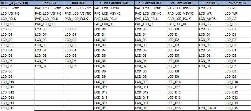
图 1‑1 视频输出接口

图 1‑2 视频输出接口
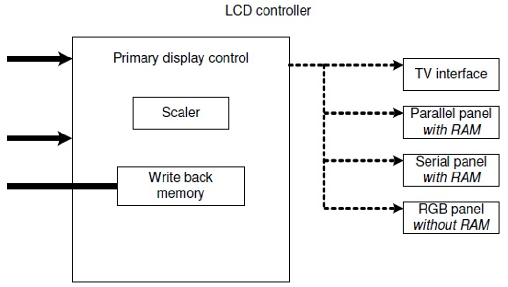
图 1‑3 Panel Control
2. Parallel Panel Control
2.1. 管脚
并行屏读写时序一般有两种模式,8080和6800。控制及传输对应的管脚为:
-
LCD_A0: High/Low to recognized index(register) or command(value) in data bus.
-
LCD_CS: LCD chip select.
8080
-
LCD_WE: LCD write enable
-
LCD_RD: LCD read enable
6800
-
LCD_RW : R/W data selection
-
E: enable
2.2. 时序
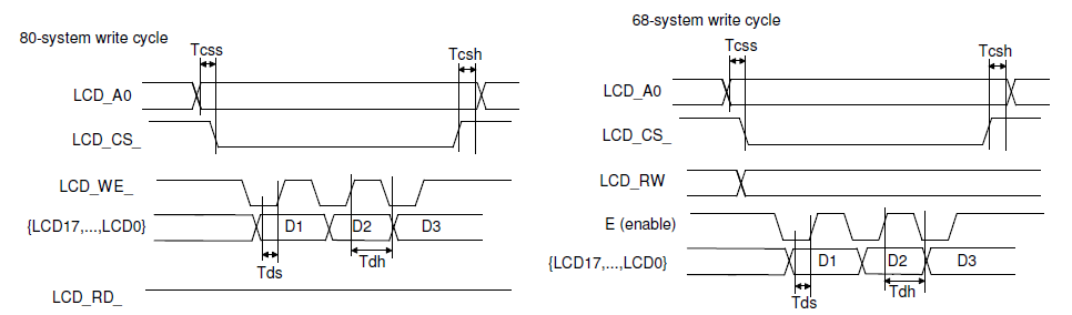
图 2‑1 8080 和 6800 写时序图

图 2‑2 8080 Burst和Non-burst模式
2.3. 调试
-
Parallel Mode: 8080 or 6800
-
Polarity of write strobe signal (Usually be low).
-
Phase of write strobe signal (Usually be rising edge latch).
-
Burst Mode or Non- burst Mode.
-
Output data bus width.
-
Output data format.
-
Output data location (The mapping between RGB and Data line)
-
Set panel size
-
Enable Panel output.
3. RGB Panel Control
3.1. 管脚
-
D/CX: Data(parameter)/command(register) selection pin. Not necessary.
-
LCD_CS(CSX): LCD chip select.
-
LCD_SDA : Communication Data pin.
-
LCD_SCL : Communication clock pin.
-
Use SPI(Serial Peripheral Interface) protocol, not I2C.
-
SPI module here means an internal function in LCD module.
3.2. 时序
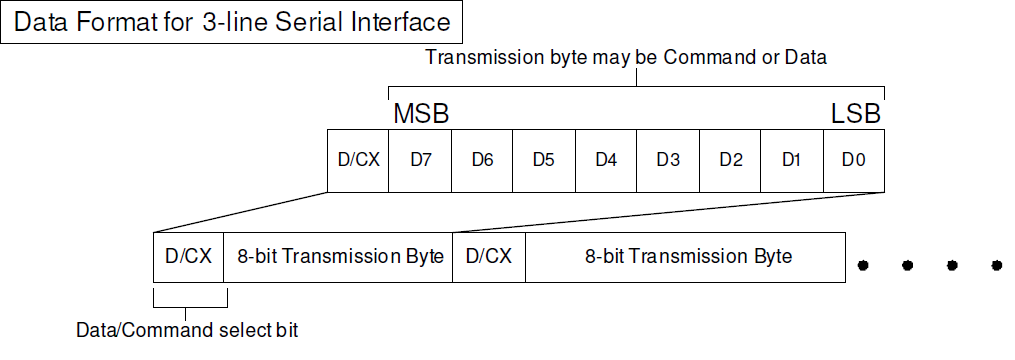
图 3‑1 数据格式
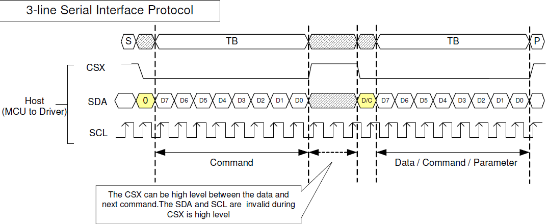
图 3‑2 时序
3.3. 调试
-
Set RGB Sync mode.
-
Turn on RGB interface clock.
-
Set the polarity of V-sync, H-sync, Clock.
-
Set Color format.
-
Set clock divider.
-
Set blanking and porch for V-sync, H-sync.
-
Set panel size
-
Setup SPI function.
3.3.1. Initial Sequence
-
Get the initial from customers.
-
Modified some items:
-
Voltage control: VCOM (for brightness and saturation)
-
Pixel format: 16/18 bits
-
Memory access control: Mirror/Flip/Rotate.
-
Gamma curve adjust.
-
Exit Sleep mode.
-
Display on.
-
4. MIPI Interface
4.1. 参数
-
1-4 Data Lanes, 1 Clock Lane
-
Level
-
LP: 0 ~ 1.2V
-
HS: 100 ~ 300mV, Common Level = 200mV, Swing = 200mV
-
-
HS: 80Mbps ~ 1.5G bps/lane (D-PHY 1.2)
4.2. 时序
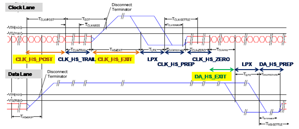
图 4‑1 Clock Lane
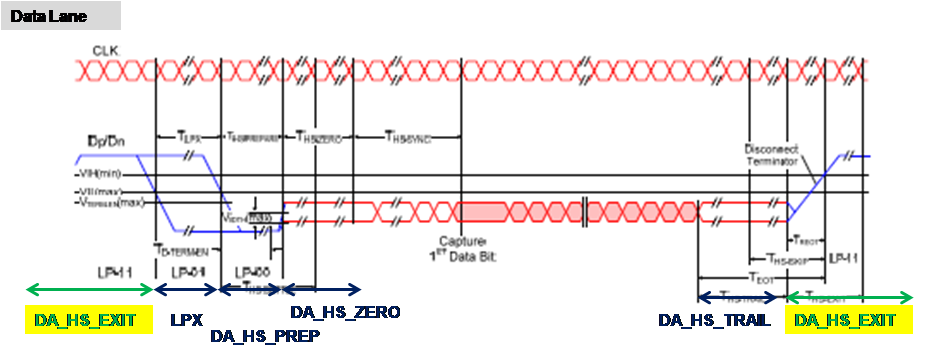
图 4‑2 Data Lane
4.3. 调试
-
Check if reset flow is correct
-
Read back register (check Lane0N/Lane0P )
- Some lcd may not provide read cmd
-
Enter lcd built-in test pattern mode if available
-
Send white display cmd to test backlight
-
Check if still in sleep-in mode
5. Debug
5.1. Tearing Effect (Parallel Output)
图 5‑1 Tearing Effect
解决方案:FLM mode
Panel output a signal(TE) to synchronize frame between MCU and LCD controller.
5.2. Effects of wrong controller settings (RGB Panel Control)

图 5‑2 正常显示

图 5‑3 RGB顺序反 (rgb --gbr)
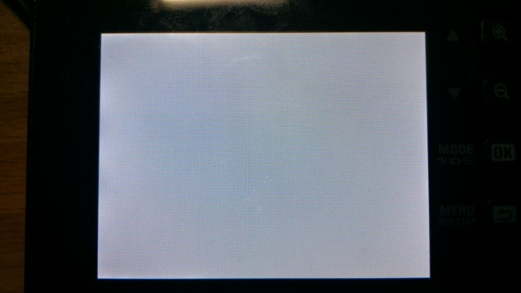
图 5‑4 白屏 (Disable delta Mode)
5.3. Color Cast (MIPI Interface)

图 5‑5 正常显示
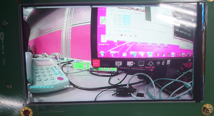
图 5‑6 偏色 (VPW/VFP不变,VBP变小)